66 www.xilinx.com Virtex-5 FPGA User Guide
UG190 (v5.0) June 19, 2009
Chapter 2: Clock Management Technology
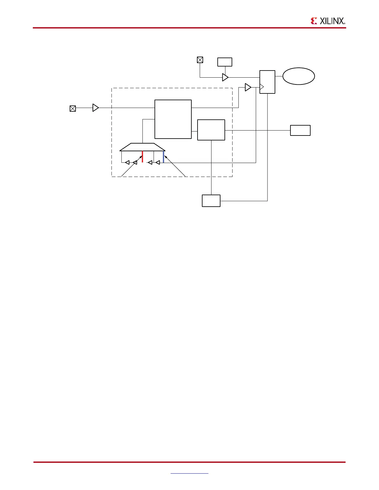
This delay element allows adjustment of the effective clock delay between the clock source
and CLK0 to guarantee non-positive hold times of IOB input flip-flop in the device.
Adding more delay to the DCM feedback path decreases the effective delay of the actual
clock path from the FPGA clock input pin to the clock input of any flip-flop. Decreasing the
clock delay increases the setup time represented in the input flip-flop, and reduces any
positive hold times required. The clock path delay includes the delay through the IBUFG,
route, DCM, BUFG, and clock-tree to the destination flip-flop. If the feedback delay equals
the clock-path delay, the effective clock-path delay is zero.
System-Synchronous Setting (Default)
By default, the feedback delay is set to system-synchronous mode. The primary timing
requirements for a system-synchronous system are non-positive hold times (or minimally
positive hold times) and minimal clock-to-out and setup times. Faster clock-to-out and
setup times allow shorter system clock periods. Ideally, the purpose of a DLL is to zero-out
the clock delay to produce faster clock-to-out and non-positive hold times. The system-
synchronous setting (default) for DESKEW_ADJUST configures the feedback delay
element to guarantee non-positive hold times for all input IOB registers. The exact delay
number added to the feedback path is device size dependent. This is determined by
characterization. In the timing report, this is included as timing reduction to input clock
path represented by the T
DCMINO
parameter. As shown in Figure 2-4, the feedback path
includes tap delays in the default setting (red line). The pin-to-pin timing parameters (with
DCM) on the Virtex-5 FPGA Data Sheet reflects the setup/hold and clock-to-out times when
the DCM is in system-synchronous mode.
In some situations, the DCM does not add this extra feedback delay, and the
DESKEW_ADJUST parameter has no effect. BitGen selects the appropriate DCM Tap
settings. These situations include:
X-Ref Target - Figure 2-4
Figure 2-4: DCM and Feedback Tap-Delay Elements
DCM
IBUFG
CLK0CLKIN
CLKFB
CLK
Source
Feedback Tap Delays
FF
DQ
Data Input
Into the
FPGA
V
CCO
DCM
Power
Regulator
V
CCINT
…
ug190_2_04_042506
V
CCAUX
System-Synchronous
Default Setting
Source-Synchronous
Setting (Delay set to zero)
 Loading...


