Virtex-5 FPGA User Guide www.xilinx.com 187
UG190 (v5.0) June 19, 2009
CLB Overview
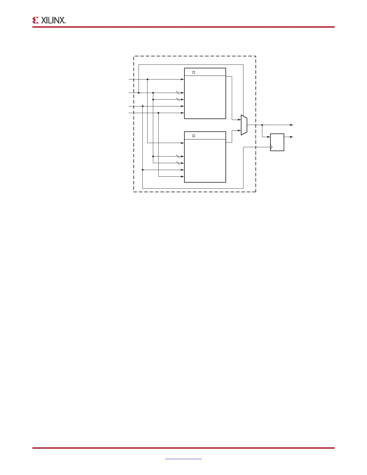
If two single-port 128 x 1-bit modules are built, the two RAM128X1S primitives can occupy
a SLICEM, as long as they share the same clock, write enable, and shared read and write
port address inputs. This configuration equates to 128 x 2-bit single-port distributed RAM.
X-Ref Target - Figure 5-12
Figure 5-12: Distributed RAM (RAM128X1S)
ug190_5_12_050506
DI1
(DX)
A6 (CX)
D
A[6:0]
WCLK
WE
(CLK)
(WE/CE)
[5:0]
[5:0]
7
SPRAM64
RAM128X1S
A[6:1]
WA[7:1]
CLK
WE
O6
DI1
7
SPRAM64
A[6:1]
WA[7:1]
CLK
WE
O6
Registered
Output
Output
F7BMUX
(Optional)
DQ
0
 Loading...


