Virtex-5 FPGA User Guide www.xilinx.com 191
UG190 (v5.0) June 19, 2009
CLB Overview
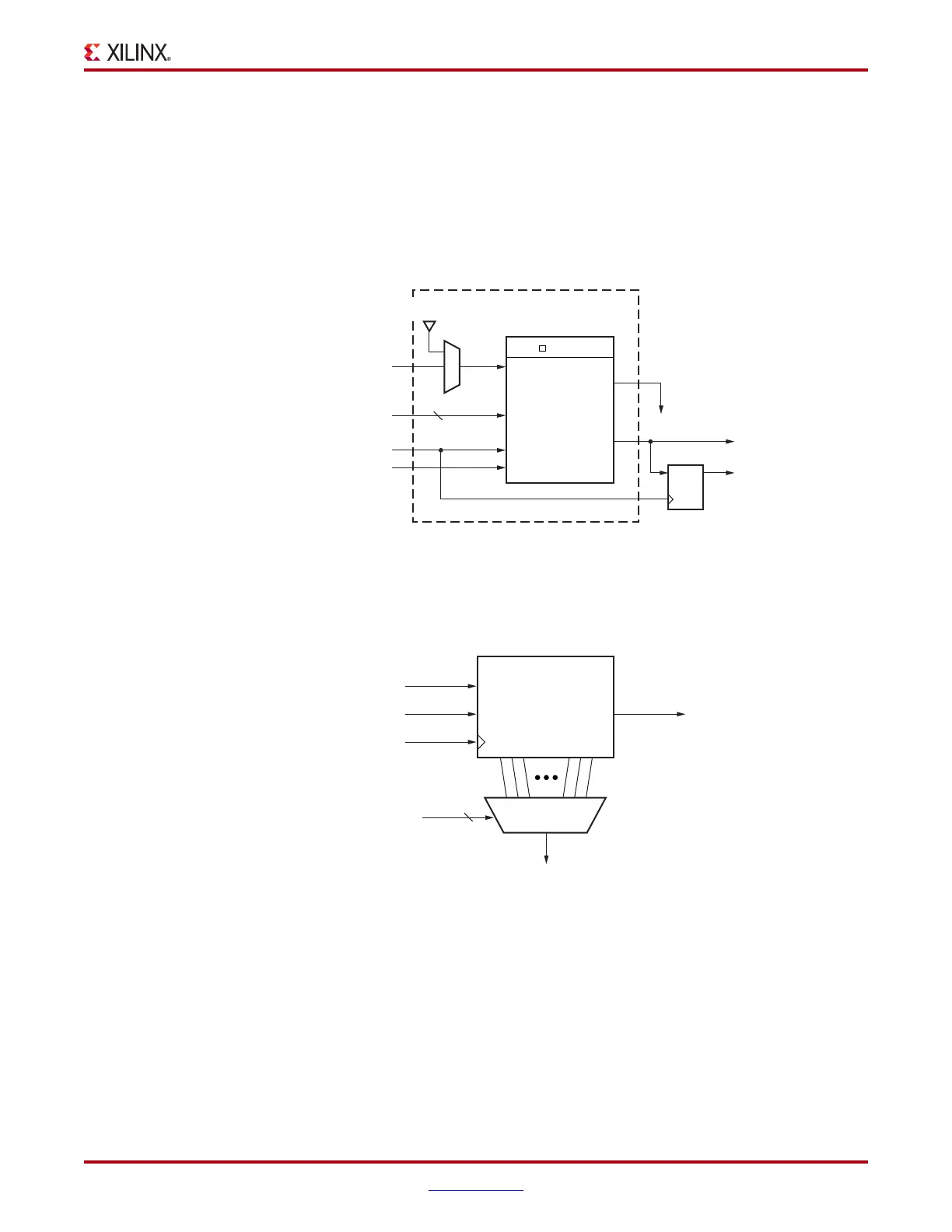
or flip-flop is available to implement a synchronous read. In this case, the clock-to-out of
the flip-flop determines the overall delay and improves performance. However, one
additional cycle of clock latency is added. Any of the 32 bits can be read out
asynchronously (at the O6 LUT outputs) by varying the 5-bit address. This capability is
useful in creating smaller shift registers (less than 32 bits). For example, when building a
13-bit shift register, simply set the address to the 13
th
bit. Figure 5-15 is a logic block
diagram of a 32-bit shift register.
Figure 5-16 illustrates an example shift register configuration occupying one function
generator.
X-Ref Target - Figure 5-15
Figure 5-15: 32-bit Shift Register Configuration
X-Ref Target - Figure 5-16
Figure 5-16: Representation of a Shift Register
ug190_5_15_050506
Output (Q)
Registered
Output
(Optional)
(AQ)
DI1
DQ
(AX)
SHIFTIN (MC31 of Previous LUT)
SHIFTIN (D)
A[4:0]
CLK
CE
(A[6:2])
(CLK)
(WE/CE)
SRL32
SRLC32E
A[6:2]
CLK
CE
O6
MC31
SHIFTOUT (Q31)
5
UG190_5_16_050506
SHIFTIN (D)
SHIFTOUT(Q31)
WE
CLK
Address (A[4:0])
32-bit Shift Register
MUX
Q
5
 Loading...


