192 www.xilinx.com Virtex-5 FPGA User Guide
UG190 (v5.0) June 19, 2009
Chapter 5: Configurable Logic Blocks (CLBs)
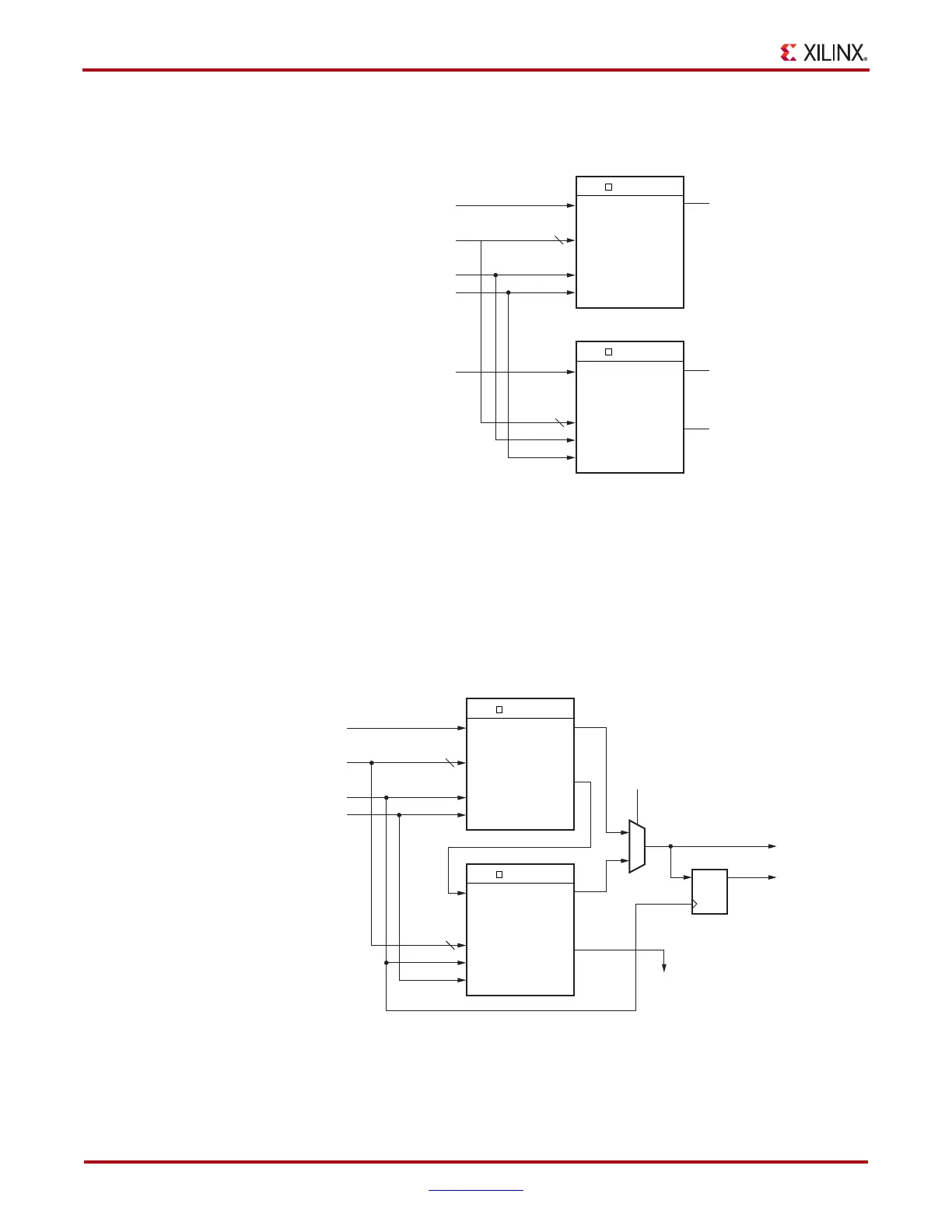
Figure 5-17 shows two 16-bit shift registers. The example shown can be implemented in a
single LUT.
As mentioned earlier, an additional output (MC31) and a dedicated connection between
shift registers allows connecting the last bit of one shift register to the first bit of the next,
without using the LUT O6 output. Longer shift registers can be built with dynamic access
to any bit in the chain. The shift register chaining and the F7AMUX, F7BMUX, and F8MUX
multiplexers allow up to a 128-bit shift register with addressable access to be implemented
in one SLICEM. Figure 5-18 through Figure 5-20 illustrate various example shift register
configurations that can occupy one SLICEM.
X-Ref Target - Figure 5-17
Figure 5-17: Dual 16-bit Shift Register Configuration
X-Ref Target - Figure 5-18
Figure 5-18: 64-bit Shift Register Configuration
UG190_5_17_050506
DI1
SHIFTIN1 (AX)
SHIFTIN2 (AI)
A[3:0]
CLK
CE
4
SRL16
A[5:2]
CLK
WE
O5
MC31
DI2
4
SRL16
A[5:2]
CLK
WE
O6
UG190_5_18_050506
DI1
SHIFTIN (D)
A[5:0]
CLK
WE
(CLK)
(WE/CE)
5
SRL32
A[6:2]
CLK
WE
O6
MC31
MC31
DI1
5
SRL32
A[6:2]
CLK
WE
O6
Registered
Output
Output (Q)
F7AMUX
(Optional)
DQ
A5 (AX)
(AQ)
SHIFTOUT (Q63)
(MC31)
 Loading...


