Virtex-5 FPGA User Guide www.xilinx.com 269
UG190 (v5.0) June 19, 2009
Specific Guidelines for I/O Supported Standards
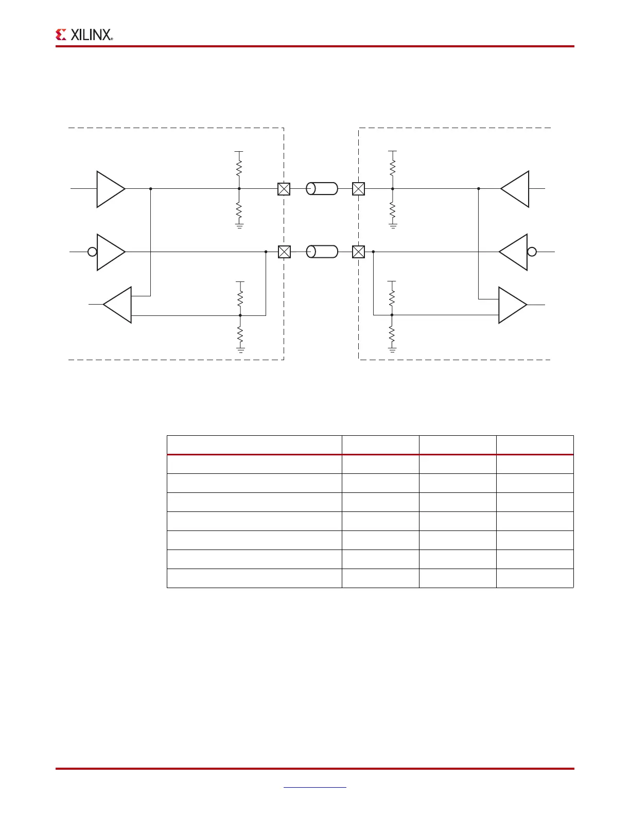
Figure 6-61 shows a sample circuit illustrating a valid termination technique for
differential HSTL Class II (1.8V) with bidirectional DCI termination.
Table 6-24 lists the differential HSTL Class II (1.8V) DC voltage specifications.
X-Ref Target - Figure 6-61
Figure 6-61: Differential HSTL (1.8V) Class II DCI Bidirectional Termination
Z
0
IOB
IOB
DIFF_HSTL_II_DCI_18 DIFF_HSTL_II_DCI_18
V
CCO
= 1.8V
2R
VRP
= 2Z
0
= 100Ω
2R
VRN
= 2Z
0
= 100Ω
+
–
DCI
V
CCO
= 1.8V
2R
VRP
= 2Z
0
= 100Ω
2R
VRN
= 2Z
0
= 100Ω
DIFF_HSTL_II_DCI_18
ug190_6_58_030306
Z
0
DIFF_HSTL_II_DCI_18
DIFF_HSTL_II_DCI_18 DIFF_HSTL_II_DCI_18
V
CCO
= 1.8V
2R
VRP
= 2Z
0
= 100Ω
2R
VRN
= 2Z
0
= 100Ω
+
–
V
CCO
= 1.8V
2R
VRP
= 2Z
0
= 100Ω
2R
VRN
= 2Z
0
= 100Ω
Table 6-24: Differential HSTL Class II (1.8V) DC Voltage Specifications
Min Typ Max
V
CCO
1.7 1.8 1.9
V
TT
– V
CCO
× 0.5 –
V
IN
(DC) –0.30 – V
CCO
+0.30
V
DIFF
(DC) 0.20 – V
CCO
+0.60
V
CM
(DC)
(1)
0.83 – 1.08
V
DIFF
(AC) 0.40 – V
CCO
+0.60
V
X
(Crossover)
(2)
0.83 – 1.08
Notes:
1. Common mode voltage: V
CM
=V
P
– ((V
P
–V
N
)/2)
2. Crossover point: V
X
where V
P
–V
N
=0 (AC coupled)
 Loading...


