30 www.xilinx.com Virtex-5 FPGA User Guide
UG190 (v5.0) June 19, 2009
Chapter 1: Clock Resources
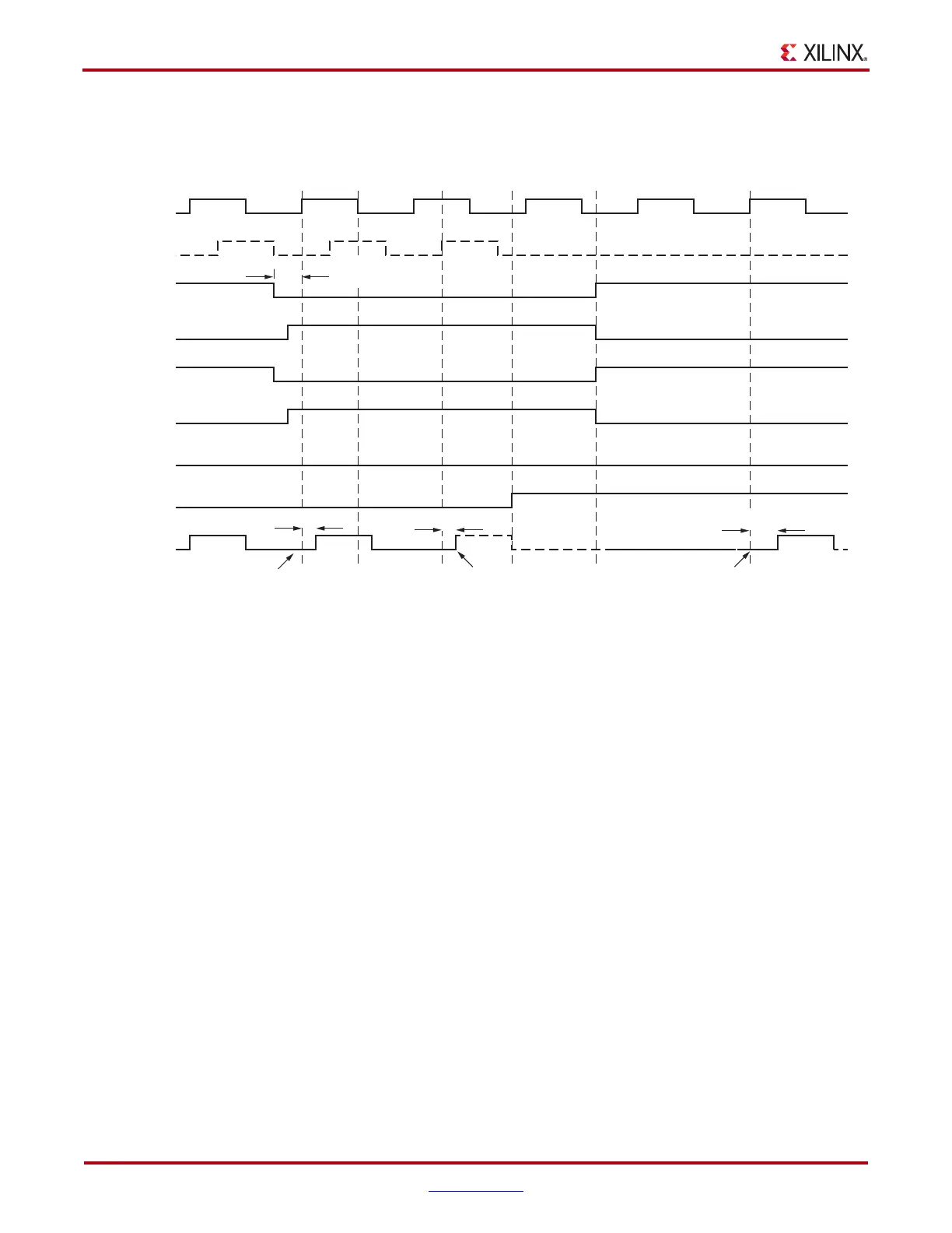
The timing diagram in Figure 1-2 illustrates various clock switching conditions using the
BUFGCTRL primitives. Exact timing numbers are best found using the speed specification.
• Before time event 1, output O uses input I0.
• At time T
BCCCK_CE
, before the rising edge at time event 1, both CE0 and S0 are
deasserted Low. At about the same time, both CE1 and S1 are asserted High.
• At time T
BCCKO_O
, after time event 3, output O uses input I1. This occurs after a High
to Low transition of I0 (event 2) followed by a High to Low transition of I1.
• At time event 4, IGNORE1 is asserted.
• At time event 5, CE0 and S0 are asserted High while CE1 and S1 are deasserted Low.
At T
BCCKO_O
, after time event 6, output O has switched from I1 to I0 without
requiring a High to Low transition of I1.
Other capabilities of BUFGCTRL are:
• Pre-selection of the I0 and I1 inputs are made after configuration but before device
operation.
• The initial output after configuration can be selected as either High or Low.
• Clock selection using CE0 and CE1 only (S0 and S1 tied High) can change the clock
selection without waiting for a High to Low transition on the previously selected
clock.
X-Ref Target - Figure 1-2
Figure 1-2: BUFGCTRL Timing Diagram
I0
I1
S0
S1
IGNORE0
IGNORE1
O
CE0
CE1
12 3 4 5 6
T
BCCCK_CE
ug190_1_02_071707
T
BCCKO_O
T
BCCKO_O
T
BCCKO_O
at I0
Begin I1
Begin I0
 Loading...


