Virtex-5 FPGA User Guide www.xilinx.com 335
UG190 (v5.0) June 19, 2009
Input/Output Delay Element (IODELAY)
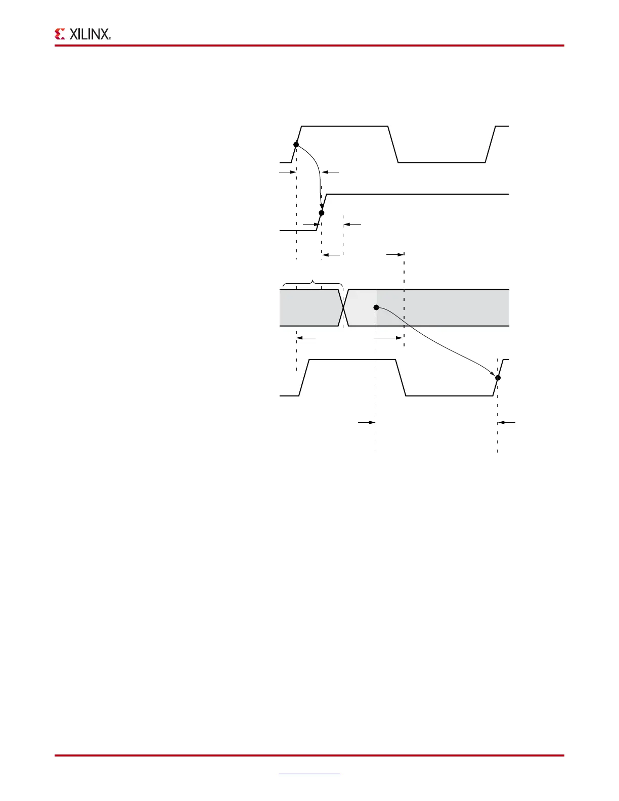
The timing diagram in Figure 7-12 shows the relevant signal timing for the case when the
I/O is an output switching to an input using 3-state control. The switching characteristics
shown in the diagram are specified in the Virtex-5 FPGA Data Sheet.
The activities of the OBUFT pin are controlled by the propagation and state of the
TSCONTROL signal from the ODDR flip-flop. The 3-state control data receipt on the
OBUF and IDDR flip-flop from a PAD are in parallel with each other, depending on the
IDELAY_VALUE setting the final value at the IDDR flip-flop input in response to a clock
edge is valid before or after the pad is driven from the 3-state control. After the 3-state
control propagates through to the PAD and the IODELAY has been switched to an input,
the IDDR setup time is the sole determiner of timing based on the IDELAY_VALUE and
other timing parameters defined in the Xilinx speed specification and represented in the
ISE tools.
X-Ref Target - Figure 7-12
Figure 7-12: Relevant Timing Signals to Examine IODELAY Timing when the IOB
Switches From an Output to an Input
IODELAY_03_082107
ODDR CLK
IDDR CLK
Pad to IDDR Setup Time is:
T
IOPI
+ T
IODDO_IDATAIN
+ T
IDOCKD
(where T
IODDO_IDATAIN
is a
function of IDELAY_VALUE)
Previous PAD
Output Value
New PAD
Input Value
TSCONTROL
PA D
ODDR CLK to
IDELAY ready
T
OCKQ
T
IOTP
T
IODDO_T
ODDR CLK to 3-state
deassertion time.
 Loading...


