Upon clearing CCIF to launch the Program Check command, the flash memory module
sets the read margin for 1s according to Table 27-30, reads the specified longword, and
compares the actual read data to the expected data provided by the FCCOB. If the
comparison at margin-1 fails, the FSTAT[MGSTAT0] bit is set.
The flash memory module then sets the read margin for 0s, re-reads, and compares again.
If the comparison at margin-0 fails, the FSTAT[MGSTAT0] bit is set. The CCIF flag is
set after the Program Check operation completes.
The supplied address must be longword aligned (the lowest two bits of the byte address
must be 00):
• Byte 3 data is written to the supplied byte address ('start'),
• Byte 2 data is programmed to byte address start+0b01,
• Byte 1 data is programmed to byte address start+0b10,
• Byte 0 data is programmed to byte address start+0b11.
NOTE
See the description of margin reads, Margin Read Commands
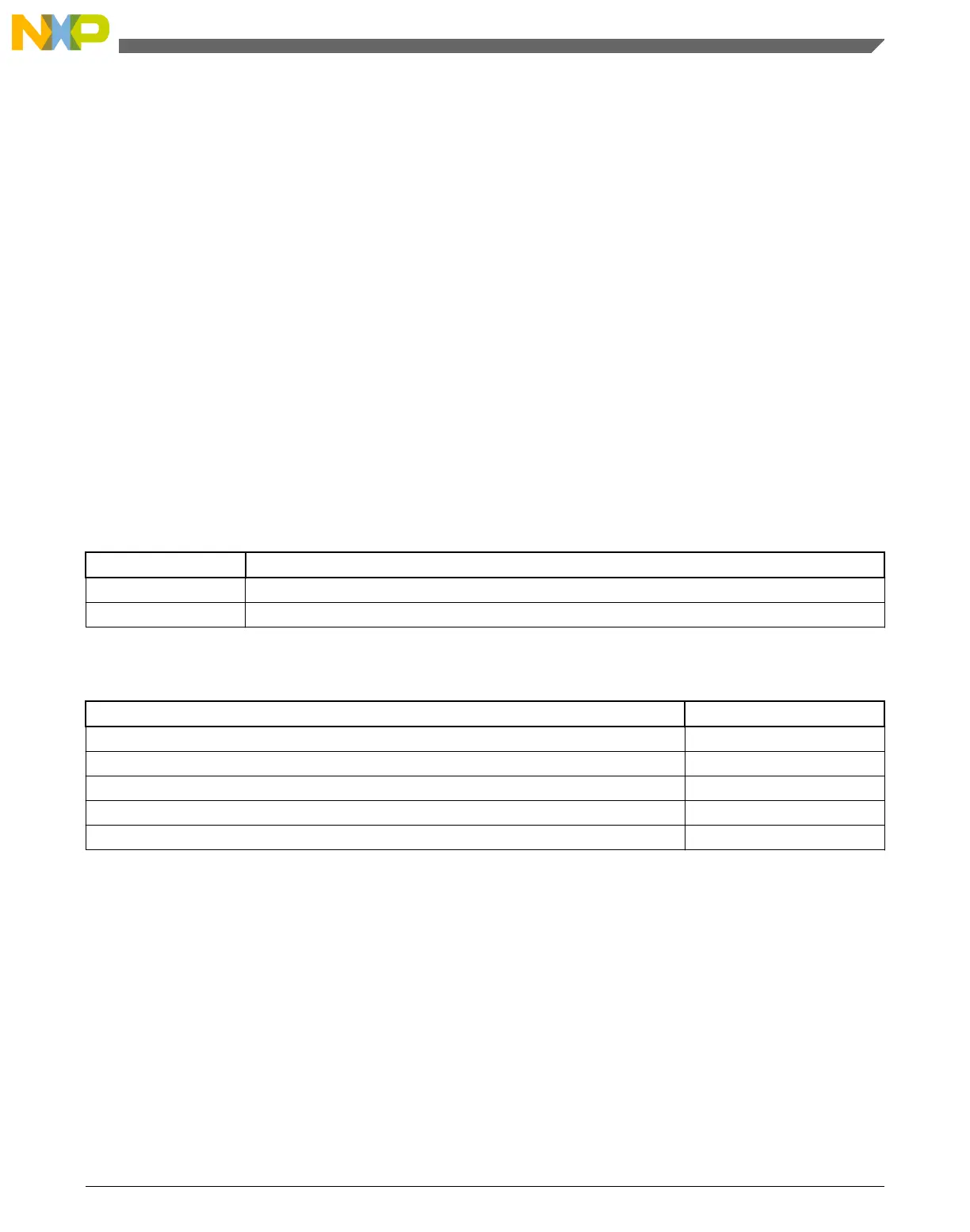
Table 27-30. Margin Level Choices for Program Check
Read Margin Choice Margin Level Description
0x01 Read at 'User' margin-1 and 'User' margin-0
0x02 Read at 'Factory' margin-1 and 'Factory' margin-0
Table 27-31. Program Check Command Error Handling
Error Condition Error Bit
Command not available in current mode/security FSTAT[ACCERR]
An invalid flash address is supplied FSTAT[ACCERR]
Flash address is not longword aligned FSTAT[ACCERR]
An invalid margin choice is supplied FSTAT[ACCERR]
Either of the margin reads does not match the expected data FSTAT[MGSTAT0]
27.4.10.3 Read Resource Command
The Read Resource command allows the user to read data from special-purpose memory
resources located within the flash memory module. The special-purpose memory
resources available include program flash IFR space and the Version ID field. Each
resource is assigned a select code as shown in Table 27-33.
Chapter 27 Flash Memory Module (FTFA)
KL25 Sub-Family Reference Manual, Rev. 3, September 2012
Freescale Semiconductor, Inc. 443

 Loading...


