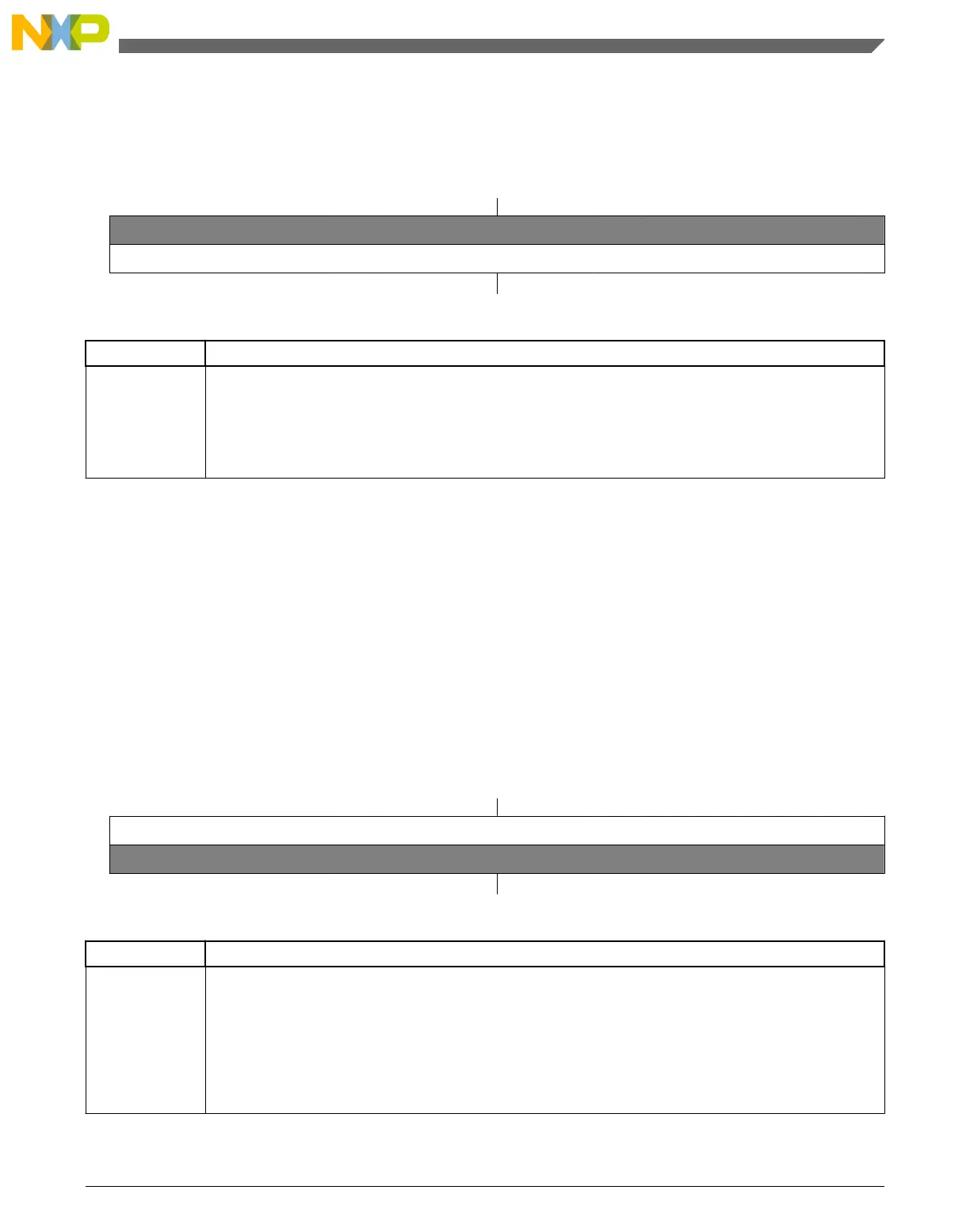
41.2.4 Port Toggle Output Register (GPIOx_PTOR)
Address: Base address + Ch offset
Bit 31 30 29 28 27 26 25 24 23 22 21 20 19 18 17 16 15 14 13 12 11 10 9 8 7 6 5 4 3 2 1 0
R
0
W
PTTO
Reset
0 0 0 0 0 0 0 0 0 0 0 0 0 0 0 0 0 0 0 0 0 0 0 0 0 0 0 0 0 0 0 0
GPIOx_PTOR field descriptions
Field Description
31–0
PTTO
Port Toggle Output
Writing to this register will update the contents of the corresponding bit in the PDOR as follows:
0 Corresponding bit in PDORn does not change.
1 Corresponding bit in PDORn is set to the inverse of its existing logic state.
41.2.5 Port Data Input Register (GPIOx_PDIR)
NOTE
Do not modify pin configuration registers associated with pins
not available in your selected package. All un-bonded pins not
available in your package will default to DISABLE state for
lowest power consumption.
Address: Base address + 10h offset
Bit 31 30 29 28 27 26 25 24 23 22 21 20 19 18 17 16 15 14 13 12 11 10 9 8 7 6 5 4 3 2 1 0
R
PDI
W
Reset
0 0 0 0 0 0 0 0 0 0 0 0 0 0 0 0 0 0 0 0 0 0 0 0 0 0 0 0 0 0 0 0
GPIOx_PDIR field descriptions
Field Description
31–0
PDI
Port Data Input
Reads 0 at the unimplemented pins for a particular device. Pins that are not configured for a digital
function read 0. If the Port Control and Interrupt module is disabled, then the corresponding bit in PDIR
does not update.
0 Pin logic level is logic 0, or is not configured for use by digital function.
1 Pin logic level is logic 1.
Chapter 41 General-Purpose Input/Output (GPIO)
KL25 Sub-Family Reference Manual, Rev. 3, September 2012
Freescale Semiconductor, Inc. 777

 Loading...


