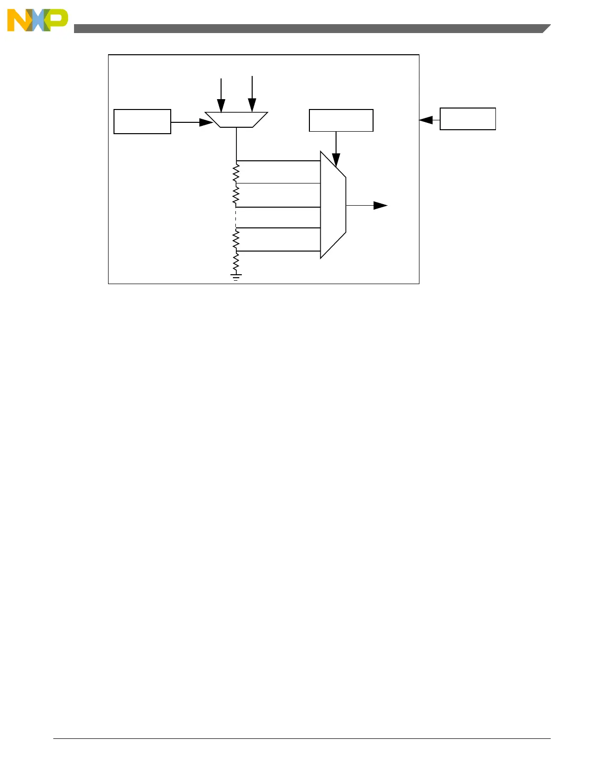
VOSEL[5:0]
DACO
MUX
MUX
DACEN
Vin
VRSEL
V
in1
V
in2
Figure 29-24. 6-bit DAC block diagram
29.13 DAC functional description
This section provides DAC functional description.
29.13.1 Voltage reference source select
• V
in1
connects to the primary voltage source as supply reference of 64 tap resistor
ladder
• V
in2
connects to an alternate voltage source
29.14 DAC resets
This module has a single reset input, corresponding to the chip-wide peripheral reset.
29.15 DAC clocks
This module has a single clock input, the bus clock.
Chapter 29 Comparator (CMP)
KL25 Sub-Family Reference Manual, Rev. 3, September 2012
Freescale Semiconductor, Inc. 535

 Loading...


