Table 3-15. Wakeup Sources
LLWU pin Module source or pin name
LLWU_P5 PTB0
LLWU_P6 PTC1
LLWU_P7 PTC3
LLWU_P8 PTC4
LLWU_P9 PTC5
LLWU_P10 PTC6
LLWU_P14 PTD4
LLWU_P15 PTD6
LLWU_M0IF LPTMR0
LLWU_M1IF CMP0
LLWU_M2IF Reserved
LLWU_M3IF Reserved
LLWU_M4IF TSI0
LLWU_M5IF RTC Alarm
LLWU_M6IF Reserved
LLWU_M7IF RTC Seconds
3.4.5 MCM Configuration
This section summarizes how the module has been configured in the chip. For a
comprehensive description of the module itself, see the module’s dedicated chapter.
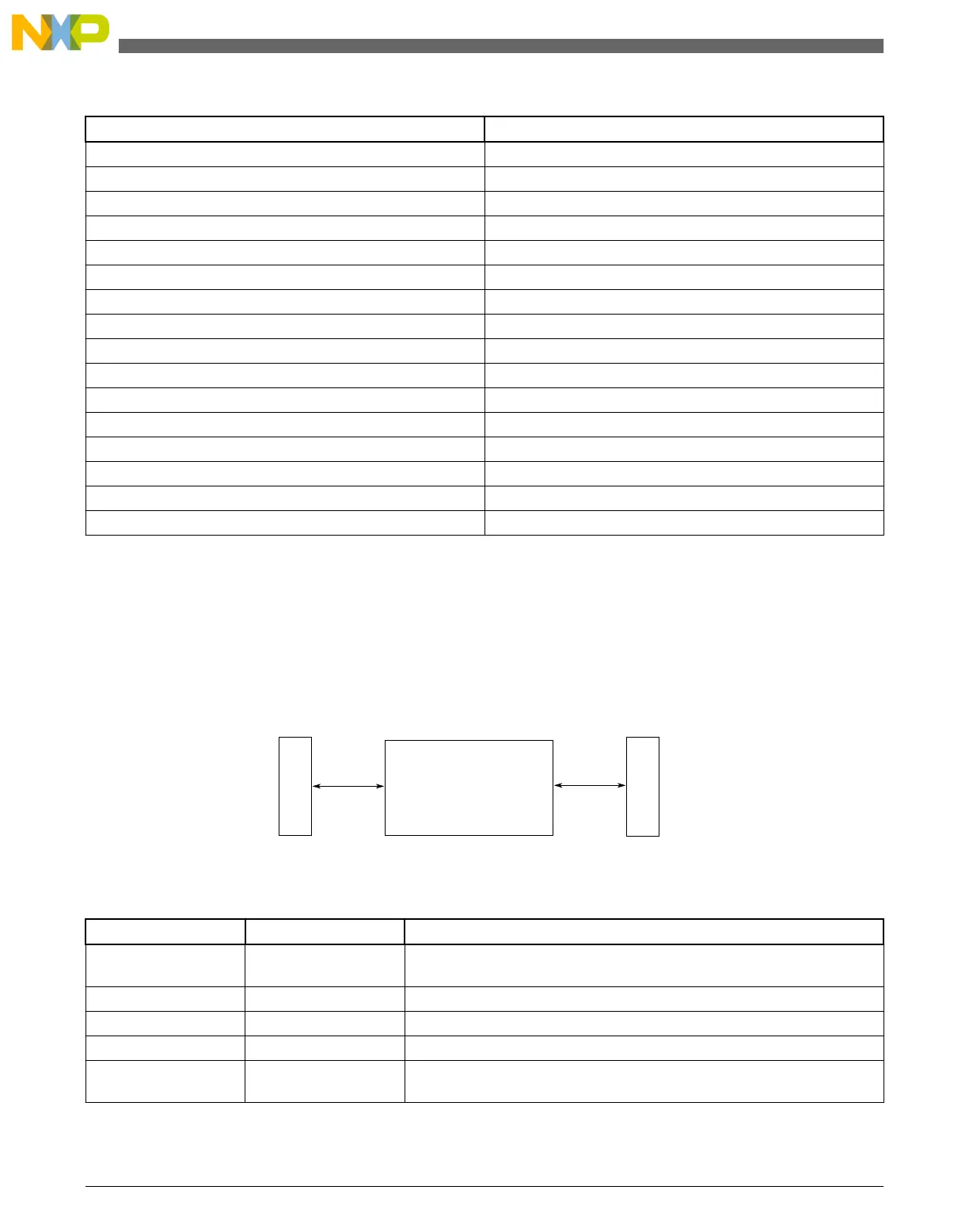
Miscellaneous
Control Module
(MCM)
Transfers
ARM Cortex-M0+
core
Flash Memory
Controller
Transfers
Figure 3-8. MCM configuration
Table 3-16. Reference links to related information
Topic Related module Reference
Full description Miscellaneous control
module (MCM)
MCM
System memory map System memory map
Clocking Clock distribution
Power management Power management
Private Peripheral Bus
(PPB)
ARM Cortex-M0+ core ARM Cortex-M0+ core
Table continues on the next page...
System Modules
KL25 Sub-Family Reference Manual, Rev. 3, September 2012
60 Freescale Semiconductor, Inc.

 Loading...


