41.1.3.1 Detailed signal description
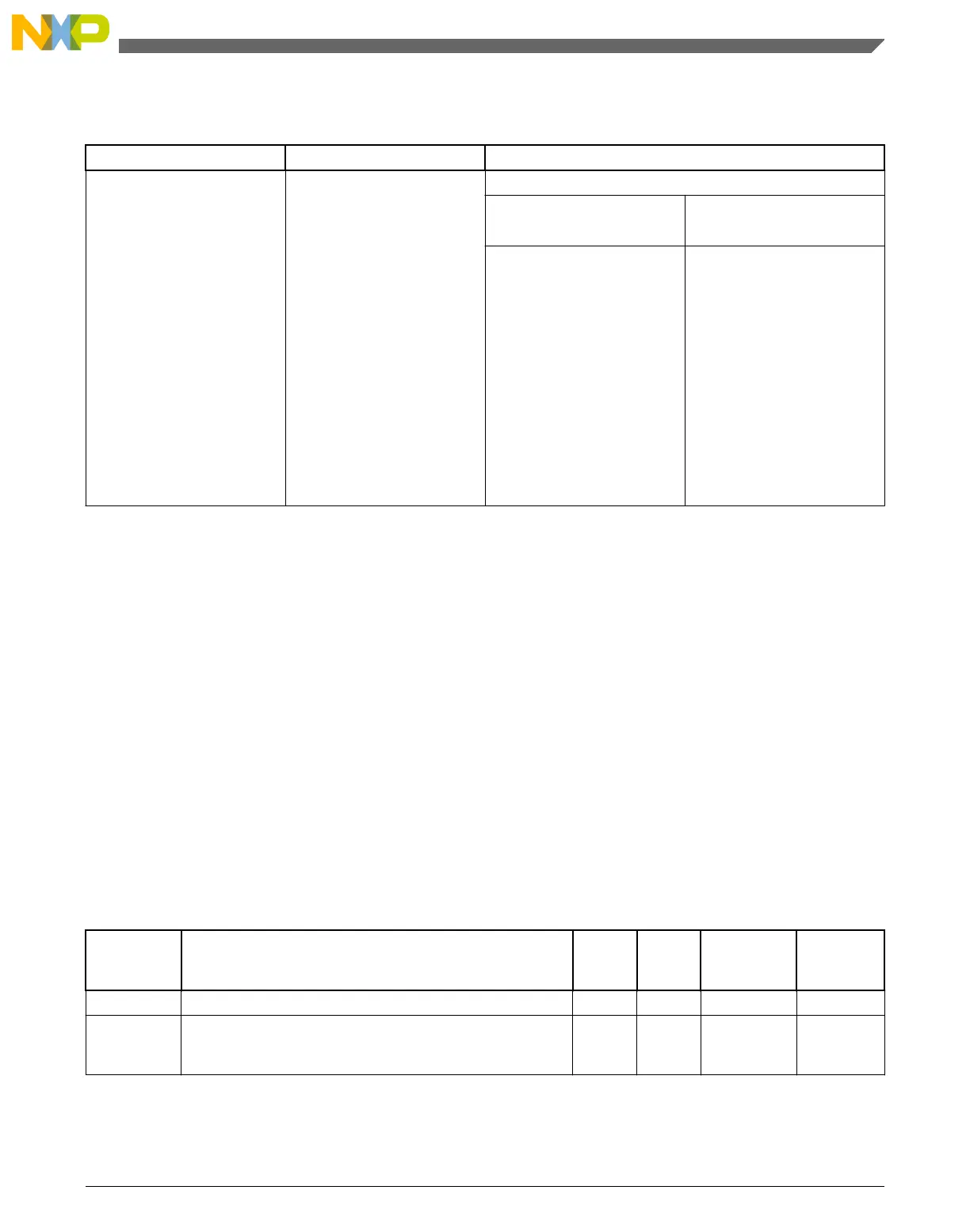
Table 41-3. GPIO interface-detailed signal descriptions
Signal I/O Description
PORTA31–PORTA0
PORTB31–PORTB0
PORTC31–PORTC0
PORTD31–PORTD0
PORTE31–PORTE0
I/O General-purpose input/output
State meaning Asserted: The pin is logic 1.
Deasserted: The pin is logic 0.
Timing Assertion: When output, this
signal occurs on the rising-
edge of the system clock. For
input, it may occur at any time
and input may be asserted
asynchronously to the system
clock.
Deassertion: When output,
this signal occurs on the
rising-edge of the system
clock. For input, it may occur
at any time and input may be
asserted asynchronously to
the system clock.
41.2 Memory map and register definition
Any read or write access to the GPIO memory space that is outside the valid memory
map results in a bus error.
NOTE
For simplicity, each GPIO port's registers appear with the same
width of 32 bits, corresponding to 32 pins. The actual number
of pins per port (and therefore the number of usable control bits
per port register) is chip-specific. Refer to the Chip
Configuration chapter to see the exact control bits for the non-
identical port instance.
GPIO memory map
Absolute
address
(hex)
Register name
Width
(in bits)
Access Reset value
Section/
page
400F_F000 Port Data Output Register (GPIOA_PDOR) 32 R/W 0000_0000h 41.2.1/775
400F_F004 Port Set Output Register (GPIOA_PSOR) 32
W
(always
reads 0)
0000_0000h 41.2.2/776
Table continues on the next page...
Chapter 41 General-Purpose Input/Output (GPIO)
KL25 Sub-Family Reference Manual, Rev. 3, September 2012
Freescale Semiconductor, Inc. 773

 Loading...


