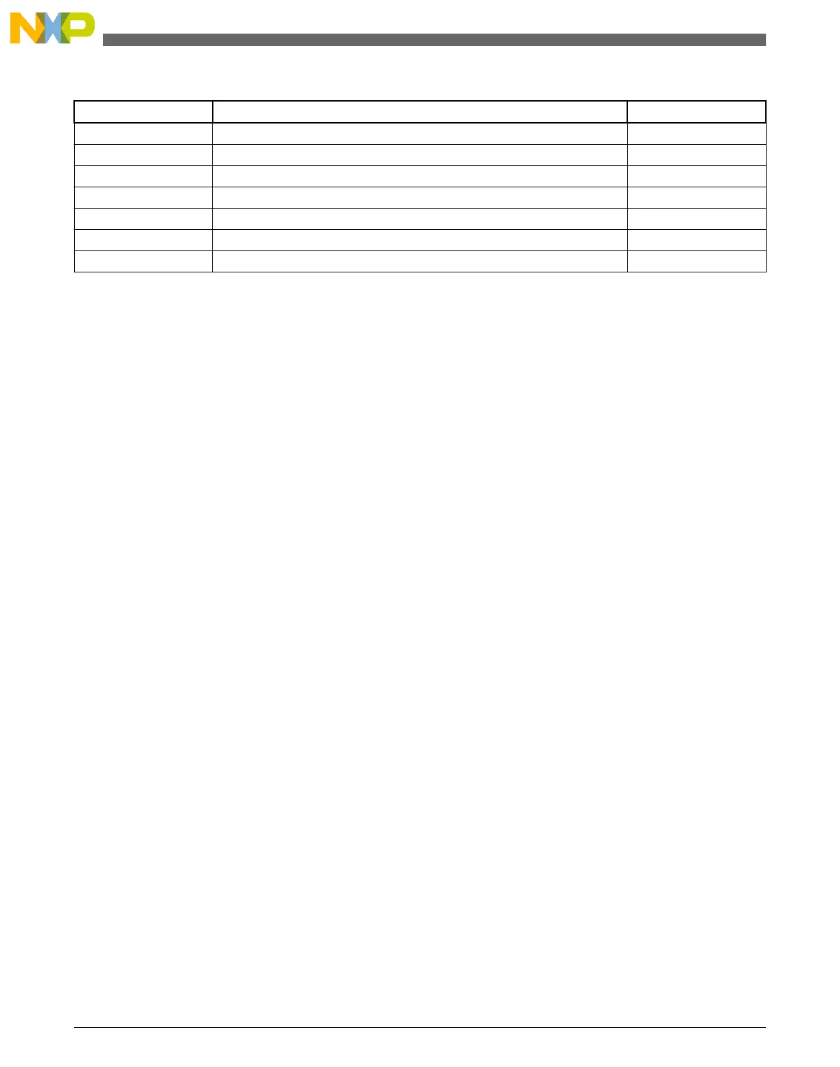
Table 28-1. ADC Signal Descriptions
Signal Description I/O
DADP3–DADP0 Differential Analog Channel Inputs I
DADM3–DADM0 Differential Analog Channel Inputs I
ADn Single-Ended Analog Channel Inputs I
V
REFSH
Voltage Reference Select High I
V
REFSL
Voltage Reference Select Low I
V
DDA
Analog Power Supply I
V
SSA
Analog Ground I
28.2.1 Analog Power (V
DDA
)
The ADC analog portion uses V
DDA
as its power connection. In some packages, V
DDA
is
connected internally to V
DD
. If externally available, connect the V
DDA
pin to the same
voltage potential as V
DD
. External filtering may be necessary to ensure clean V
DDA
for
good results.
28.2.2 Analog Ground (V
SSA
)
The ADC analog portion uses V
SSA
as its ground connection. In some packages, V
SSA
is
connected internally to V
SS
. If externally available, connect the V
SSA
pin to the same
voltage potential as V
SS
.
28.2.3 Voltage Reference Select
V
REFSH
and V
REFSL
are the high and low reference voltages for the ADC module.
The ADC can be configured to accept one of two voltage reference pairs for V
REFSH
and
V
REFSL
. Each pair contains a positive reference that must be between the minimum Ref
Voltage High and V
DDA
, and a ground reference that must be at the same potential as
V
SSA
. The two pairs are external (V
REFH
and V
REFL
) and alternate (V
ALTH
and V
ALTL
).
These voltage references are selected using SC2[REFSEL]. The alternate V
ALTH
and
V
ALTL
voltage reference pair may select additional external pins or internal sources
depending on MCU configuration. See the chip configuration information on the Voltage
References specific to this MCU.
ADC Signal Descriptions
KL25 Sub-Family Reference Manual, Rev. 3, September 2012
460 Freescale Semiconductor, Inc.

 Loading...


