3.5.2 OSC Configuration
This section summarizes how the module has been configured in the chip. For a
comprehensive description of the module itself, see the module’s dedicated chapter.
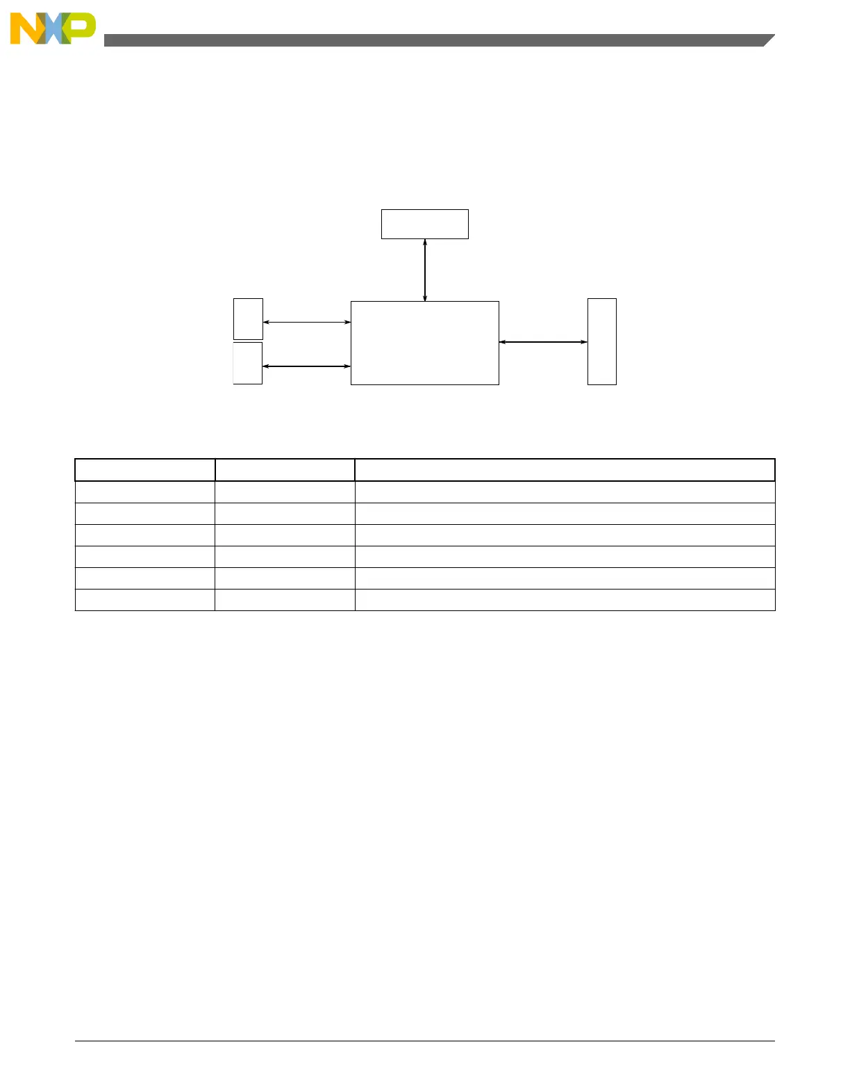
Signal multiplexing
Register
access
Peripheral
bridge
System oscillator
MCG
Module signals
RTC
Figure 3-15. OSC configuration
Table 3-25. Reference links to related information
Topic Related module Reference
Full description OSC OSC
System memory map System memory map
Clocking Clock distribution
Power management Power management
Signal multiplexing Port control Signal multiplexing
Full description MCG MCG
3.5.2.1 OSC modes of operation with MCG and RTC
The most common method of controlling the OSC block is through MCG clock source
selection MCG_C1[CLKS] and the MCG_C2 register bits to configure the oscillator
frequency range, gain-mode, and for crystal or external clock operation. The OSC_CR
also provides control for enabling the OSC and configuring internal load capacitors for
the EXTAL and XTAL pins. See the OSC and MCG chapters for more details.
The RTC_CR[OSCE] bit has overriding control over the MCG and OSC_CR enable
functions. When RTC_CR[OSCE] is set, the OSC is configured for low frequency, low
power and the RTC_CR[SCxP] bits override the OSC_CR[SCxP] bits to control the
internal capacitance configuration. See the RTC chapter for more details.
Chapter 3 Chip Configuration
KL25 Sub-Family Reference Manual, Rev. 3, September 2012
Freescale Semiconductor, Inc. 71

 Loading...


