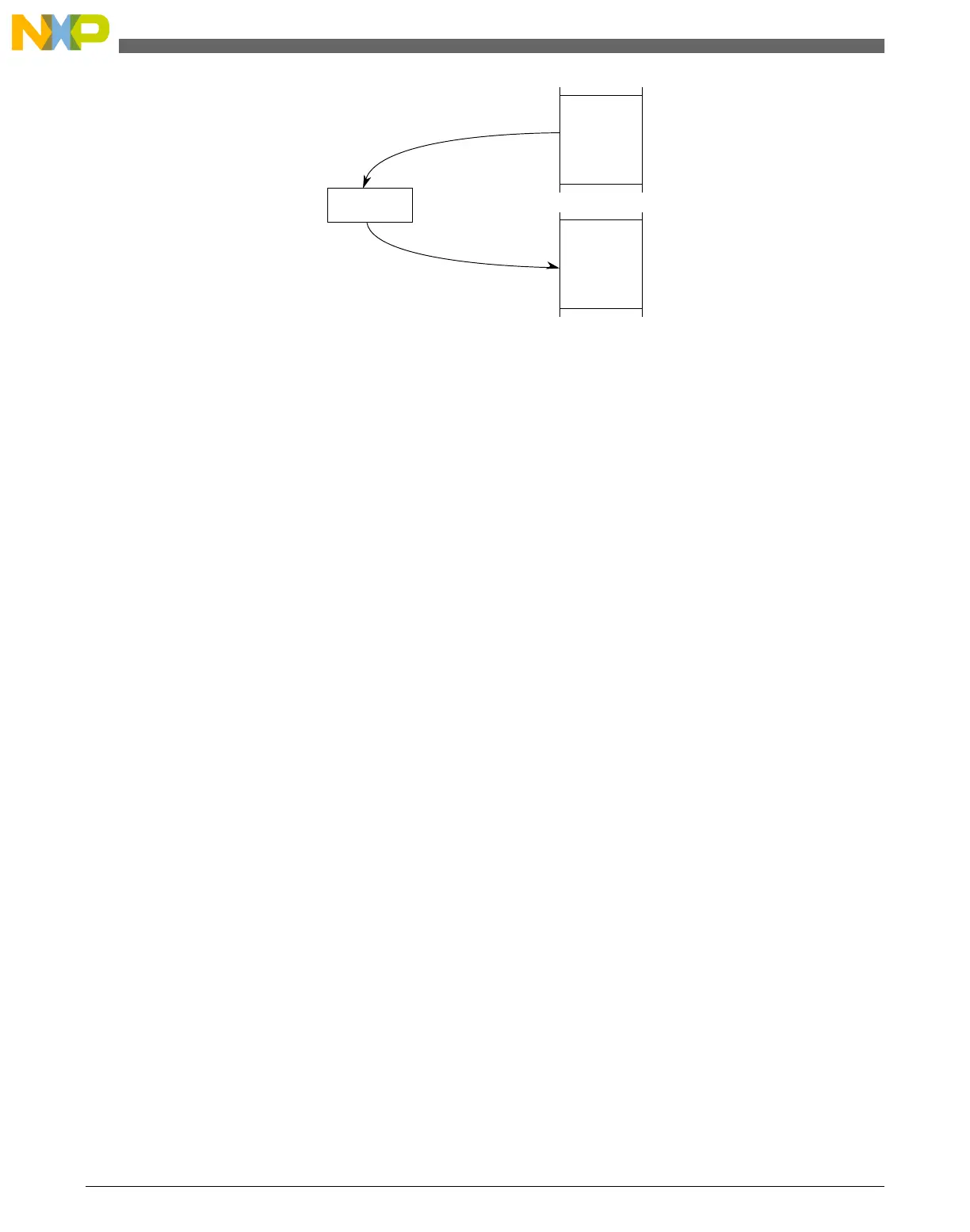
Control and Data
Write
Read
DMA
Memory/
Peripheral
Memory/
Peripheral
Control and Data
Figure 23-2. Dual-Address Transfer
Any operation involving a DMA channel follows the same three steps:
1. Channel initialization—The transfer control descriptor, contained in the channel
registers, is loaded with address pointers, a byte-transfer count, and control
information using accesses from the slave peripheral bus.
2. Data transfer—The DMA accepts requests for data transfers. Upon receipt of a
request, it provides address and bus control for the transfers via its master connection
to the system bus and temporary storage for the read data. The channel performs one
or more source read and destination write data transfers.
3. Channel termination—Occurs after the operation is finished successfully or due to an
error. The channel indicates the operation status in the channel's DSR, described in
the definitions of the DMA Status Registers (DSRn) and Byte Count Registers
(BCRn).
Memory Map and Registers
Descriptions of each register and its bit assignments follow. Modifying DMA control
registers during a transfer can result in undefined operation. The following table shows
the mapping of DMA controller registers. The DMA programming model is accessed via
the slave peripheral bus. The concatenation of the source and destination address
registers, the status and byte count register, and the control register create a 128-bit
transfer control descriptor (TCD) that defines the operation of each DMA channel.
23.3
Memory Map and Registers
KL25 Sub-Family Reference Manual, Rev. 3, September 2012
352 Freescale Semiconductor, Inc.

 Loading...


