37.3.6 SPI match register (SPIx_M)
This register contains the hardware compare value. When the value received in the SPI
receive data buffer equals this hardware compare value, the SPI match flag (SPMF) sets.
Address: 4007_6000h base + 7h offset = 4007_6007h
Bit 7 6 5 4 3 2 1 0
Read
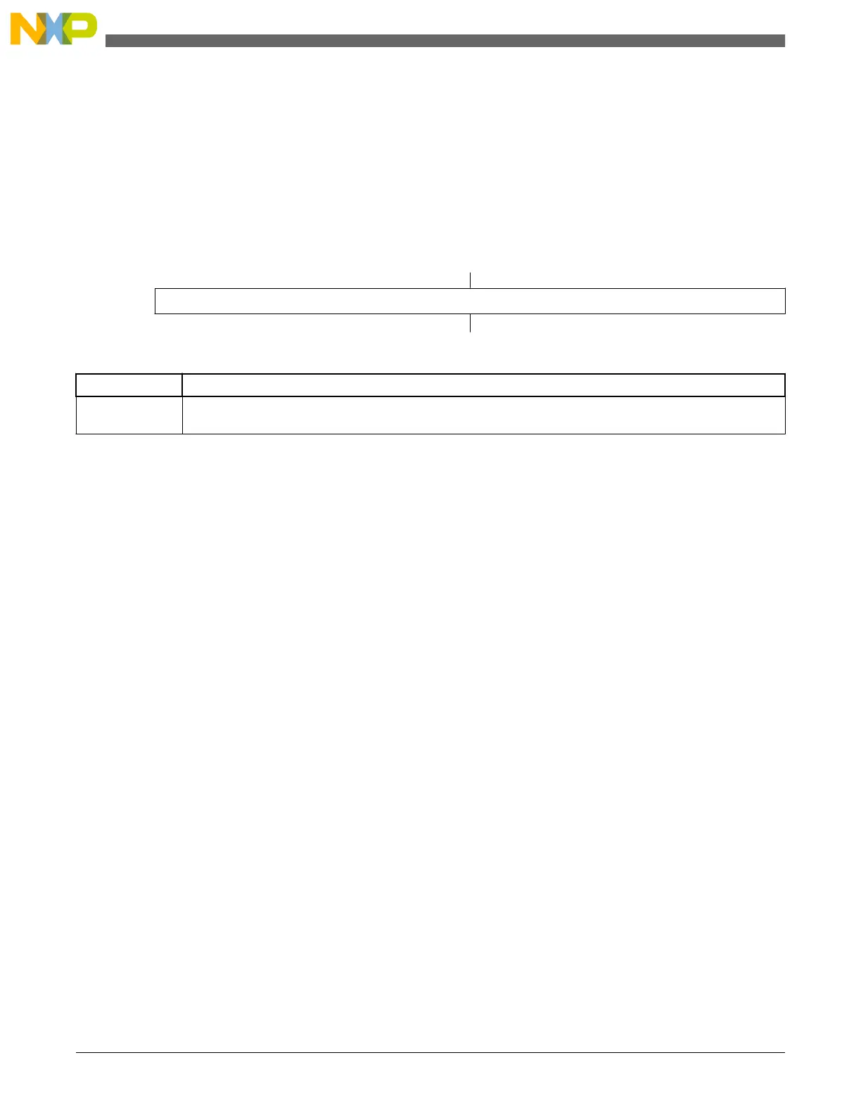
Bits[7:0]
Write
Reset
0 0 0 0 0 0 0 0
SPI0_M field descriptions
Field Description
7–0
Bits[7:0]
Hardware compare value (low byte)
37.4 Functional Description
This section provides the functional description of the module.
37.4.1 General
The SPI system is enabled by setting the SPI enable (SPE) bit in SPI Control Register 1.
While the SPE bit is set, the four associated SPI port pins are dedicated to the SPI
function as:
• Slave select (SS)
• Serial clock (SPSCK)
• Master out/slave in (MOSI)
• Master in/slave out (MISO)
An SPI transfer is initiated in the master SPI device by reading the SPI status register
(SPIx_S) when SPTEF = 1 and then writing data to the transmit data buffer (write to
SPIxD ). When a transfer is complete, received data is moved into the receive data buffer.
The SPIxD register acts as the SPI receive data buffer for reads and as the SPI transmit
data buffer for writes.
Functional Description
KL25 Sub-Family Reference Manual, Rev. 3, September 2012
668 Freescale Semiconductor, Inc.

 Loading...


