10.4.5 Analog
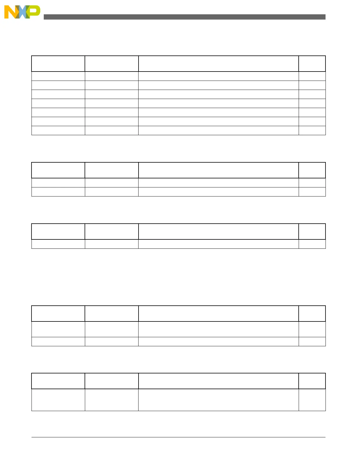
Table 10-6. ADC 0 Signal Descriptions
Chip signal name Module signal
name
Description I/O
ADC0_DPn DADP3–DADP0 Differential Analog Channel Inputs I
ADC0_DMn DADM3–DADM0 Differential Analog Channel Inputs I
ADC0_SEn ADn Single-Ended Analog Channel Inputs I
VREFH V
REFSH
Voltage Reference Select High I
VREFL V
REFSL
Voltage Reference Select Low I
VDDA V
DDA
Analog Power Supply I
VSSA V
SSA
Analog Ground I
Table 10-7. CMP 0 Signal Descriptions
Chip signal name Module signal
name
Description I/O
CMP0_IN[5:0] IN[5:0] Analog voltage inputs I
CMP0_OUT CMPO Comparator output O
Table 10-8. DAC 0 Signal Descriptions
Chip signal name Module signal
name
Description I/O
DAC0_OUT — DAC output O
10.4.6 Timer Modules
Table 10-9. TPM 0 Signal Descriptions
Chip signal name Module signal
name
Description I/O
TPM_CLKIN[2:0] EXTCLK External clock. FTM external clock can be selected to drive the
FTM counter.
I
TPM0_CH[5:0] CHn FTM channel (n), where n can be 7-0 I/O
Table 10-10. TPM 1 Signal Descriptions
Chip signal name Module signal
name
Description I/O
TPM_CLKIN[2:0] TPM_EXTCLK External clock. TPM external clock can be selected to increment the
TPM counter on every rising edge synchronized to the counter
clock.
I
Table continues on the next page...
Module Signal Description Tables
KL25 Sub-Family Reference Manual, Rev. 3, September 2012
170 Freescale Semiconductor, Inc.

 Loading...


