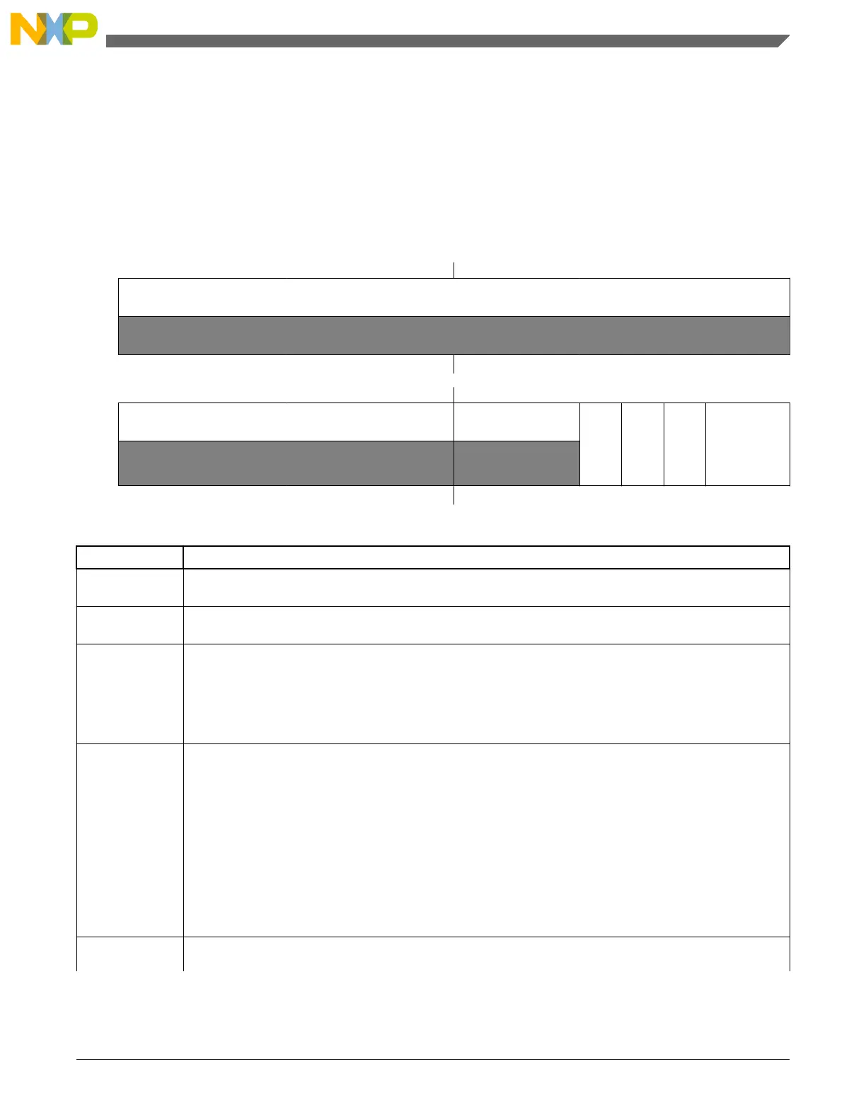
28.3.3 ADC Configuration Register 2 (ADCx_CFG2)
Configuration Register 2 (CFG2) selects the special high-speed configuration for very
high speed conversions and selects the long sample time duration during long sample
mode.
Address: 4003_B000h base + Ch offset = 4003_B00Ch
Bit 31 30 29 28 27 26 25 24 23 22 21 20 19 18 17 16
R
0
W
Reset
0 0 0 0 0 0 0 0 0 0 0 0 0 0 0 0
Bit
15 14 13 12 11 10 9 8 7 6 5 4 3 2 1 0
R
0 0
MUXSEL
ADACKEN
ADHSC
ADLSTS
W
Reset
0 0 0 0 0 0 0 0 0 0 0 0 0 0 0 0
ADCx_CFG2 field descriptions
Field Description
31–8
Reserved
This field is reserved.
This read-only field is reserved and always has the value 0.
7–5
Reserved
This field is reserved.
This read-only field is reserved and always has the value 0.
4
MUXSEL
ADC Mux Select
Changes the ADC mux setting to select between alternate sets of ADC channels.
0 ADxxa channels are selected.
1 ADxxb channels are selected.
3
ADACKEN
Asynchronous Clock Output Enable
Enables the asynchronous clock source and the clock source output regardless of the conversion and
status of CFG1[ADICLK]. Based on MCU configuration, the asynchronous clock may be used by other
modules. See chip configuration information. Setting this field allows the clock to be used even while the
ADC is idle or operating from a different clock source. Also, latency of initiating a single or first-continuous
conversion with the asynchronous clock selected is reduced because the ADACK clock is already
operational.
0 Asynchronous clock output disabled; Asynchronous clock is enabled only if selected by ADICLK and a
conversion is active.
1 Asynchronous clock and clock output is enabled regardless of the state of the ADC.
2
ADHSC
High-Speed Configuration
Table continues on the next page...
Chapter 28 Analog-to-Digital Converter (ADC)
KL25 Sub-Family Reference Manual, Rev. 3, September 2012
Freescale Semiconductor, Inc. 467

 Loading...


