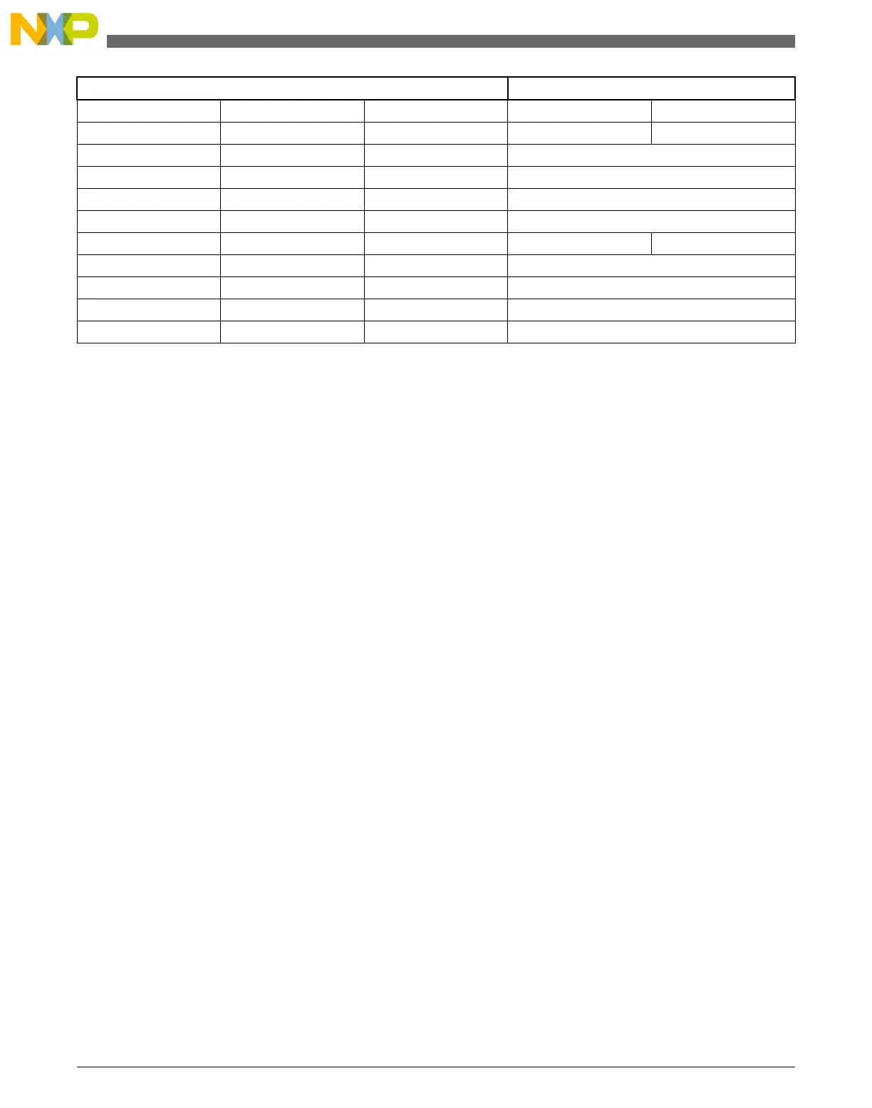
ADC configuration Sample time (ADCK cycles)
CFG1[ADLSMP] CFG2[ADLSTS] CFG2[ADHSC] First or Single Subsequent
0 X 0 6 4
1 00 0 24
1 01 0 16
1 10 0 10
1 11 0 6
0 X 1 8 6
1 00 1 26
1 01 1 18
1 10 1 12
1 11 1 8
The total conversion time depends upon:
• The sample time as determined by CFG1[ADLSMP] and CFG2[ADLSTS]
• The MCU bus frequency
• The conversion mode, as determined by CFG1[MODE] and SC1n[DIFF]
• The high speed configuration, that is, CFG2[ADHSC]
• The frequency of the conversion clock, that is, f
ADCK
.
CFG2[ADHSC] is used to configure a higher clock input frequency. This will allow
faster overall conversion times. To meet internal ADC timing requirements,
CFG2[ADHSC] adds additional ADCK cycles. Conversions with CFG2[ADHSC]=1 take
two more ADCK cycles. CFG2[ADHSC] must be used when the ADCLK exceeds the
limit for CFG2[ADHSC]=0.
After the module becomes active, sampling of the input begins.
1. CFG1[ADLSMP] and CFG2[ADLSTS] select between sample times based on the
conversion mode that is selected.
2. When sampling is completed, the converter is isolated from the input channel and a
successive approximation algorithm is applied to determine the digital value of the
analog signal.
3. The result of the conversion is transferred to Rn upon completion of the conversion
algorithm.
If the bus frequency is less than f
ADCK
, precise sample time for continuous conversions
cannot be guaranteed when short sample is enabled, that is, when CFG1[ADLSMP]=0.
The maximum total conversion time is determined by the clock source chosen and the
divide ratio selected. The clock source is selectable by CFG1[ADICLK], and the divide
ratio is specified by CFG1[ADIV].
Functional description
KL25 Sub-Family Reference Manual, Rev. 3, September 2012
488 Freescale Semiconductor, Inc.

 Loading...


