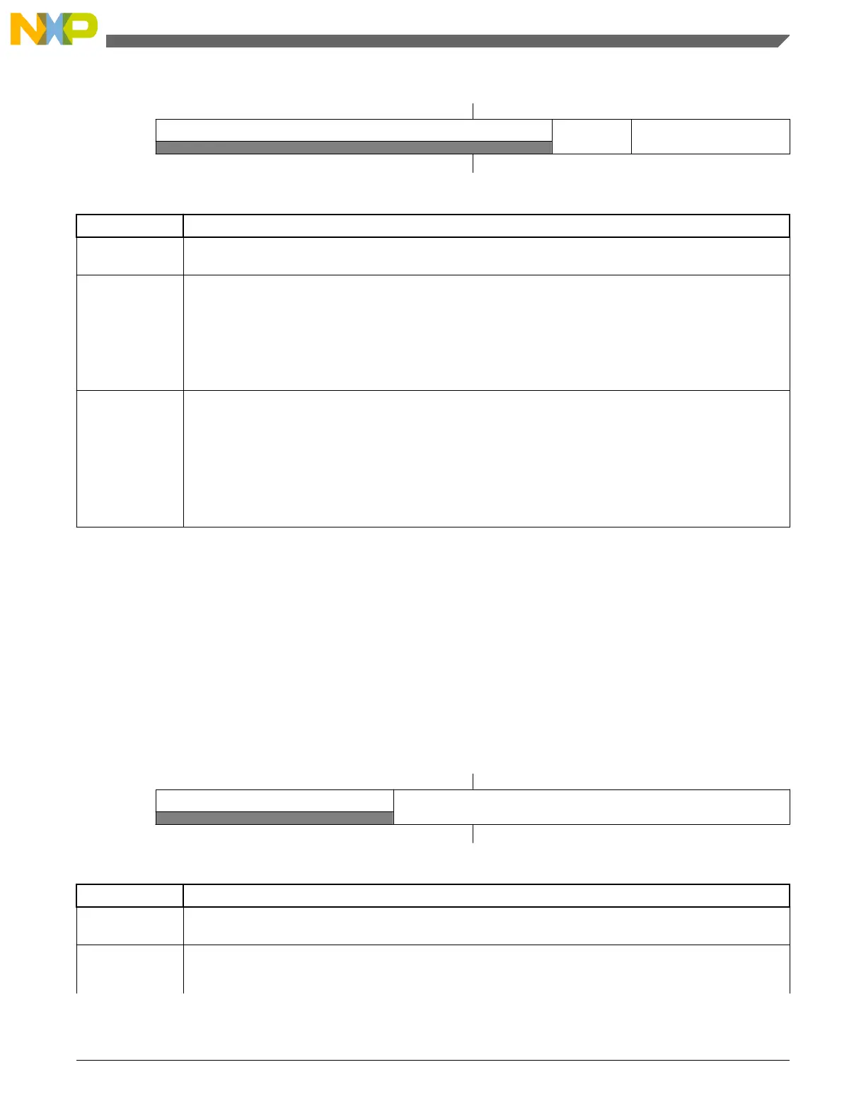
Address: 4007_F000h base + 4h offset = 4007_F004h
Bit 7 6 5 4 3 2 1 0
Read 0
RSTFLTSS RSTFLTSRW
Write
Reset
0 0 0 0 0 0 0 0
RCM_RPFC field descriptions
Field Description
7–3
Reserved
This field is reserved.
This read-only field is reserved and always has the value 0.
2
RSTFLTSS
Reset Pin Filter Select in Stop Mode
Selects how the reset pin filter is enabled in Stop and VLPS modes , and also during LLS and VLLS
modes. On exit from VLLS mode, this bit should be reconfigured before clearing ACKISO in the PMC.
0 All filtering disabled
1 LPO clock filter enabled
1–0
RSTFLTSRW
Reset Pin Filter Select in Run and Wait Modes
Selects how the reset pin filter is enabled in run and wait modes.
00 All filtering disabled
01 Bus clock filter enabled for normal operation
10 LPO clock filter enabled for normal operation
11 Reserved
16.2.4 Reset Pin Filter Width register (RCM_RPFW)
NOTE
The reset values of the bits in the RSTFLTSEL field are for
Chip POR only. They are unaffected by other reset types.
Address: 4007_F000h base + 5h offset = 4007_F005h
Bit 7 6 5 4 3 2 1 0
Read 0
RSTFLTSEL
Write
Reset
0 0 0 0 0 0 0 0
RCM_RPFW field descriptions
Field Description
7–5
Reserved
This field is reserved.
This read-only field is reserved and always has the value 0.
4–0
RSTFLTSEL
Reset Pin Filter Bus Clock Select
Selects the reset pin bus clock filter width.
Table continues on the next page...
Chapter 16 Reset Control Module (RCM)
KL25 Sub-Family Reference Manual, Rev. 3, September 2012
Freescale Semiconductor, Inc. 269

 Loading...


