ENABLE
SPI SYSTEM
SHIFT
OUT
SHIFT
DIRECTION
SHIFT
CLOCK
Rx BUFFER
FULL
Tx BUFFER
EMPTY
SHIFT
IN
Tx BUFFER (WRITE SPIxD)
SPI SHIFT REGISTER
Rx BUFFER (READ SPIxD)
PIN CONTROL
MASTER CLOCK
SLAVE CLOCK
BUS RATE
CLOCK
SPIBR
CLOCK GENERATOR
MASTER/SLAVE
MODE SELECT
CLOCK
LOGIC
MODE FAULT
DETECTION
RX DMA DONE
Rx_DMA REQ
TX DMA DONE
TX DMA REQ
8-BIT COMPARATOR
SPIxM
MASTER/
SLAVE
SPSCK
SS
S
M
S
M
S
M
MOSI
(MOMI)
MISO
(SISO)
INTERRUPT
REQUEST
SPE
LSBFE
MSTR
SPMF
SPMIE
SPTIE
SPIE
MODF
TXDMAE
RXDMAE
SPRF
SPTEF
MOD-
SSOE
SPC0
BIDIROE
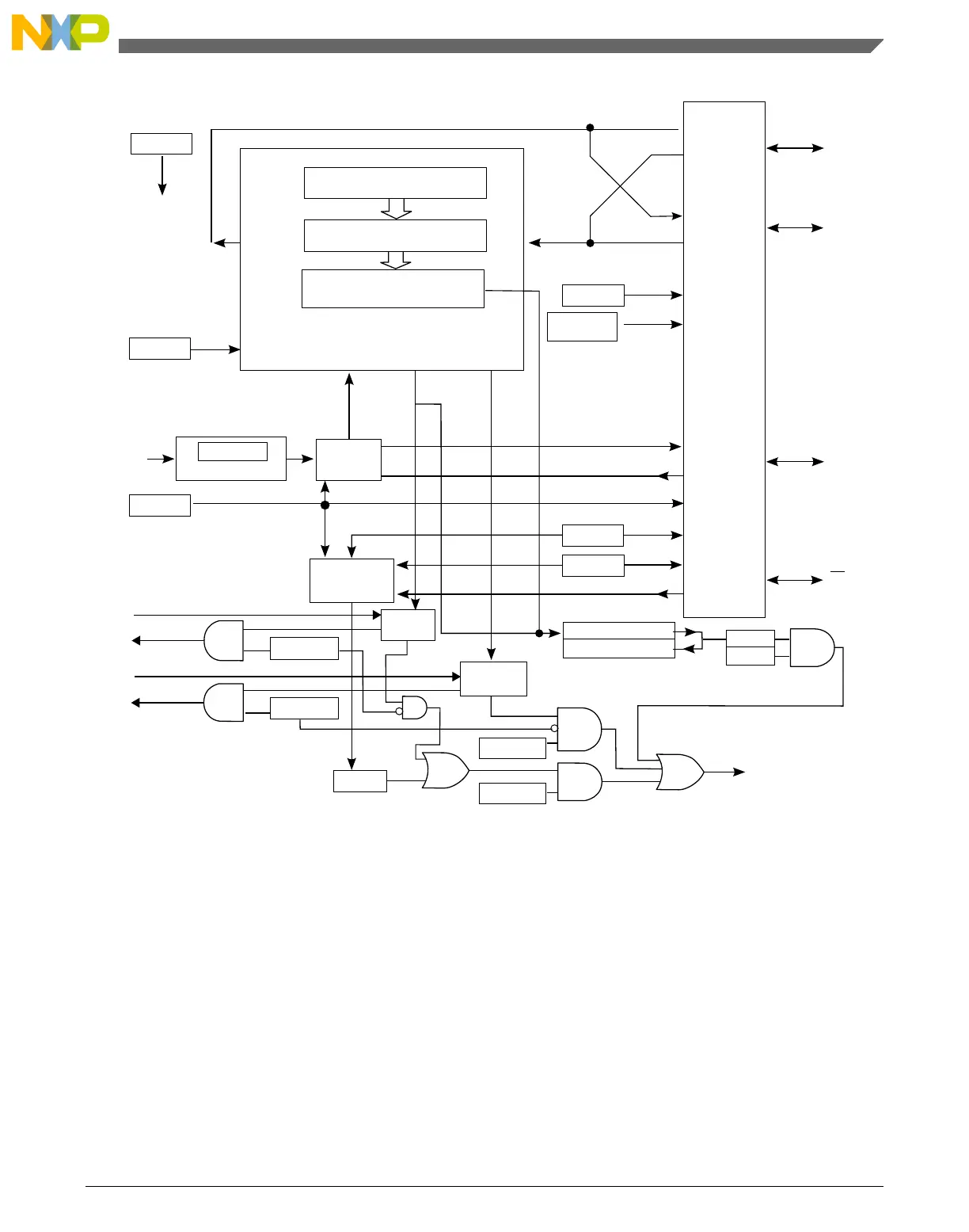
Figure 37-2. SPI Module Block Diagram without FIFO
37.2 External Signal Description
The SPI optionally shares four port pins. The function of these pins depends on the
settings of SPI control bits. When the SPI is disabled (SPE = 0), these four pins revert to
other functions that are not controlled by the SPI (based on chip configuration).
Chapter 37 Serial Peripheral Interface (SPI)
KL25 Sub-Family Reference Manual, Rev. 3, September 2012
Freescale Semiconductor, Inc. 659

 Loading...


