ADCx_SC2 field descriptions (continued)
Field Description
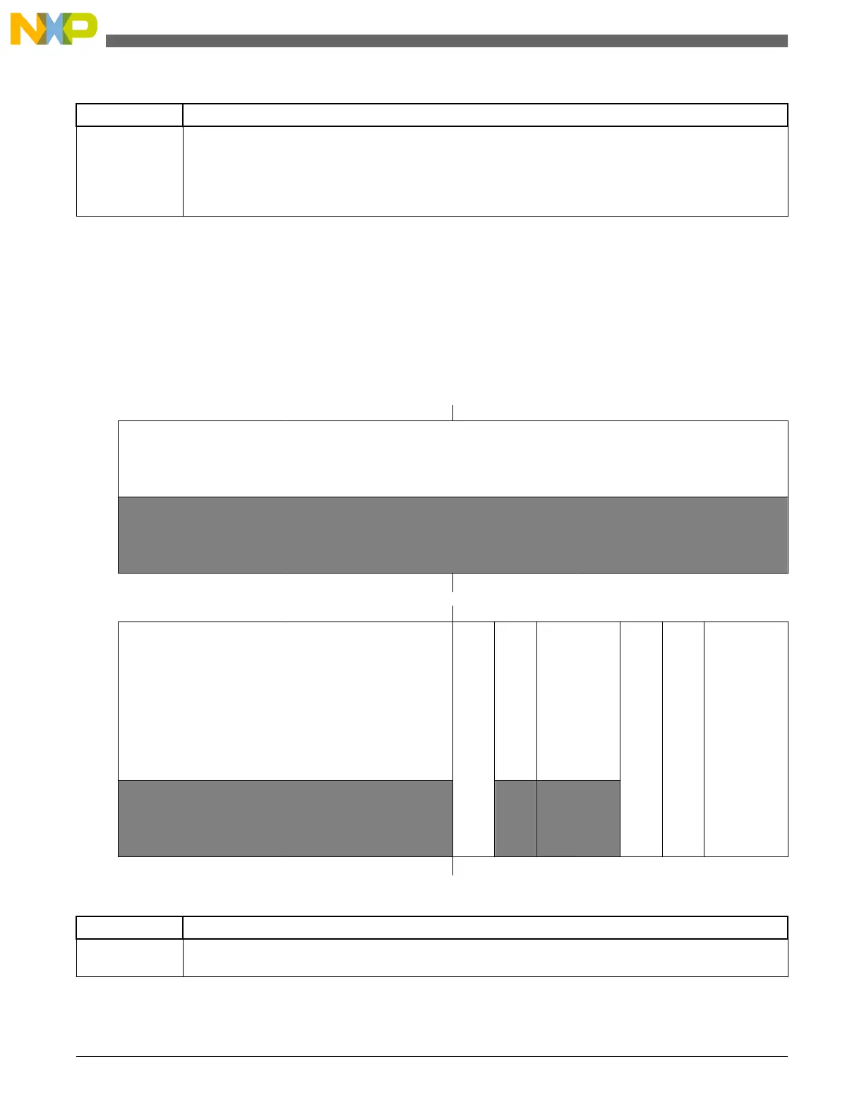
01 Alternate reference pair, that is, V
ALTH
and V
ALTL
. This pair may be additional external pins or
internal sources depending on the MCU configuration. See the chip configuration information for
details specific to this MCU
10 Reserved
11 Reserved
28.3.7 Status and Control Register 3 (ADCx_SC3)
The Status and Control Register 3 (SC3) controls the calibration, continuous convert, and
hardware averaging functions of the ADC module.
Address: 4003_B000h base + 24h offset = 4003_B024h
Bit 31 30 29 28 27 26 25 24 23 22 21 20 19 18 17 16
R
0
W
Reset
0 0 0 0 0 0 0 0 0 0 0 0 0 0 0 0
Bit
15 14 13 12 11 10 9 8 7 6 5 4 3 2 1 0
R
0
CAL
CALF
0
ADCO
AVGE
AVGS
W
Reset
0 0 0 0 0 0 0 0 0 0 0 0 0 0 0 0
ADCx_SC3 field descriptions
Field Description
31–8
Reserved
This field is reserved.
This read-only field is reserved and always has the value 0.
Table continues on the next page...
Register definition
KL25 Sub-Family Reference Manual, Rev. 3, September 2012
472 Freescale Semiconductor, Inc.

 Loading...


