Interrupt
Write/Read
Address
SCL
SDA
Module Enable
CTRL_REG
DATA_MUX
ADDR_DECODE
DATA_REGSTATUS_REGADDR_REGFREQ_REG
Input
Sync
Clock
Control
START
STOP
Arbitration
Control
In/Out
Data
Shift
Register
Address
Compare
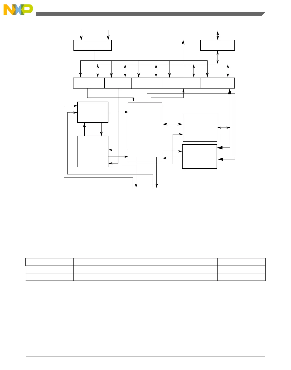
Figure 38-1. I2C Functional block diagram
38.2 I
2
C signal descriptions
The signal properties of I
2
C are shown in the following table.
Table 38-1. I
2
C signal descriptions
Signal Description I/O
SCL Bidirectional serial clock line of the I
2
C system. I/O
SDA Bidirectional serial data line of the I
2
C system. I/O
Memory map and register descriptions
This section describes in detail all I2C registers accessible to the end user.
38.3
Chapter 38 Inter-Integrated Circuit (I2C)
KL25 Sub-Family Reference Manual, Rev. 3, September 2012
Freescale Semiconductor, Inc. 689

 Loading...


