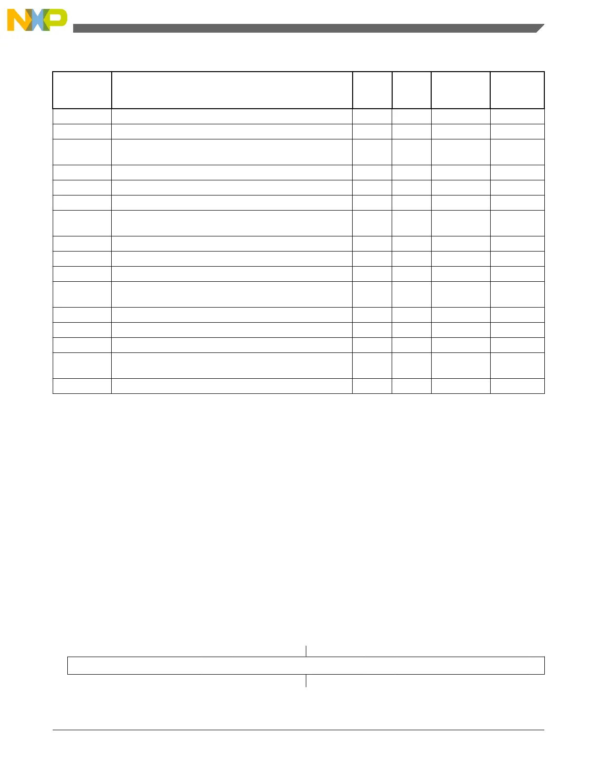
DMA memory map
Absolute
address
(hex)
Register name
Width
(in bits)
Access Reset value
Section/
page
4000_8100 Source Address Register (DMA_SAR0) 32 R/W 0000_0000h 23.3.1/353
4000_8104 Destination Address Register (DMA_DAR0) 32 R/W 0000_0000h 23.3.2/354
4000_8108
DMA Status Register / Byte Count Register
(DMA_DSR_BCR0)
32 R/W 0000_0000h 23.3.3/355
4000_810C DMA Control Register (DMA_DCR0) 32 R/W 0000_0000h 23.3.4/357
4000_8110 Source Address Register (DMA_SAR1) 32 R/W 0000_0000h 23.3.1/353
4000_8114 Destination Address Register (DMA_DAR1) 32 R/W 0000_0000h 23.3.2/354
4000_8118
DMA Status Register / Byte Count Register
(DMA_DSR_BCR1)
32 R/W 0000_0000h 23.3.3/355
4000_811C DMA Control Register (DMA_DCR1) 32 R/W 0000_0000h 23.3.4/357
4000_8120 Source Address Register (DMA_SAR2) 32 R/W 0000_0000h 23.3.1/353
4000_8124 Destination Address Register (DMA_DAR2) 32 R/W 0000_0000h 23.3.2/354
4000_8128
DMA Status Register / Byte Count Register
(DMA_DSR_BCR2)
32 R/W 0000_0000h 23.3.3/355
4000_812C DMA Control Register (DMA_DCR2) 32 R/W 0000_0000h 23.3.4/357
4000_8130 Source Address Register (DMA_SAR3) 32 R/W 0000_0000h 23.3.1/353
4000_8134 Destination Address Register (DMA_DAR3) 32 R/W 0000_0000h 23.3.2/354
4000_8138
DMA Status Register / Byte Count Register
(DMA_DSR_BCR3)
32 R/W 0000_0000h 23.3.3/355
4000_813C DMA Control Register (DMA_DCR3) 32 R/W 0000_0000h 23.3.4/357
23.3.1 Source Address Register (DMA_SARn)
Restriction
For this register:
• Only 32-bit writes are allowed. 16-bit and 8-bit writes
result in a bus error.
• Only four values are allowed to be written to bits 31-20 of
this register. A write of any other value to these bits causes
a configuration error when the channel starts to execute.
For more information about the configuration error, see the
description of the CE field of DSR.
Address: 4000_8000h base + 100h offset + (16d × i), where i=0d to 3d
Bit 31 30 29 28 27 26 25 24 23 22 21 20 19 18 17 16 15 14 13 12 11 10 9 8 7 6 5 4 3 2 1 0
R
SAR
W
Reset
0 0 0 0 0 0 0 0 0 0 0 0 0 0 0 0 0 0 0 0 0 0 0 0 0 0 0 0 0 0 0 0
Chapter 23 DMA Controller Module
KL25 Sub-Family Reference Manual, Rev. 3, September 2012
Freescale Semiconductor, Inc. 353

 Loading...


