Signal multiplexing
Module signals
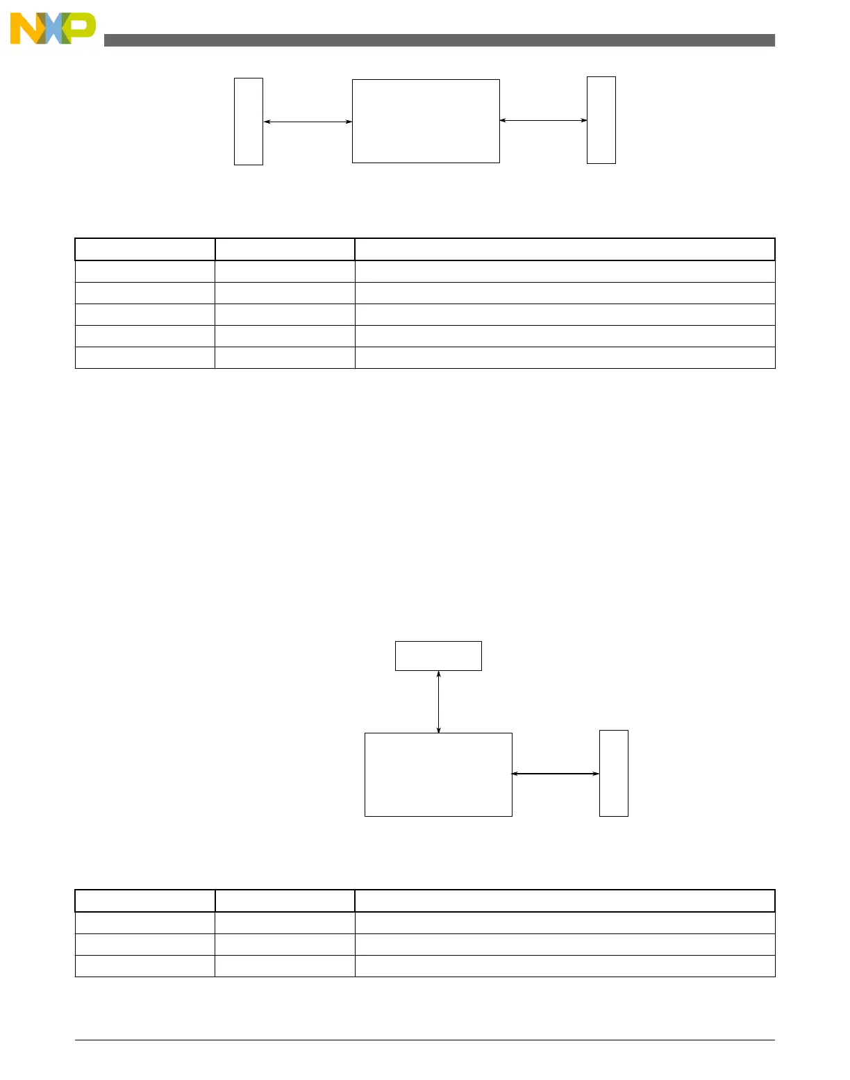
USB Voltage
Regulator
USB OTG
Figure 3-33. USB Voltage Regulator configuration
Table 3-44. Reference links to related information
Topic Related module Reference
Full description USB Voltage Regulator USB Voltage Regulator
System memory map System memory map
Clocking Clock Distribution
USB controller USB controller
Signal Multiplexing Port control Signal Multiplexing
NOTE
When USB is not used in the application, it is recommended
that the USB regulator VREGIN and VOUT33 pins remain
floating.
3.9.2 SPI configuration
This section summarizes how the module has been configured in the chip. For a
comprehensive description of the module itself, see the module’s dedicated chapter.
Signal multiplexing
Register
access
SPI
Peripheral
bridge
Module signals
Figure 3-34. SPI configuration
Table 3-45. Reference links to related information
Topic Related module Reference
Full description SPI SPI
System memory map System memory map
Clocking Clock Distribution
Table continues on the next page...
Communication interfaces
KL25 Sub-Family Reference Manual, Rev. 3, September 2012
96 Freescale Semiconductor, Inc.

 Loading...


