The MCU uses the FTFA_FOPT register bits to configure the device at reset as shown in
the following table.
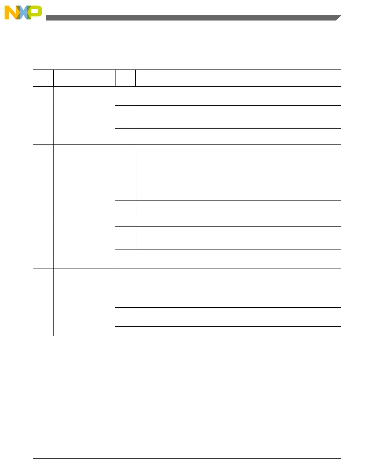
Table 6-2. Flash Option Register (FTFA_FOPT) Bit Definitions
Bit
Num
Field Value Definition
7-6 Reserved Reserved for future expansion.
5 FAST_INIT Select initialization speed on POR, VLLSx, and any system reset .
0 Slower initialization. The Flash initialization will be slower with the benefit of
reduced average current during this time. The duration of the recovery will be
controlled by the clock divider selection determined by the LPBOOT setting.
1 Fast Initialization.The Flash has faster recoveries at the expense of higher current
during these times.
3 RESET_PIN_CFG Enable/disable control for the RESET pin.
0 RESET pin is disabled following a POR and cannot be enabled as RESET
function. When this option is selected, there could be a short period of contention
during a POR ramp where the device drives the pin out low prior to establishing the
setting of this option and releasing the RESET function on the pin.
This bit is preserved through system resets and low power modes. When RESET
pin function is disabled it cannot be used as a source for low power mode wakeup.
1 RESET pin is dedicated. The port is configured with pullup enabled, open drain,
passive filter enabled.
2 NMI_DIS Enable/disable control for the NMI function.
0 NMI interrupts are always blocked. The associated pin continues to default to NMI
pin controls with internal pullup enabled. When NMI pin function is disabled it
cannot be used as a source for low power mode wakeup.
1 NMI pin/interrupts reset default to enabled.
1 Reserved Reserved for future expansion.
4,0 LPBOOT Control the reset value of OUTDIV1 value in SIM_CLKDIV1 register. Larger divide value
selections produce lower average power consumption during POR, VLLSx recoveries and
reset sequencing and after reset exit. The recovery times are also extended if the
FAST_INIT option is not selected.
00 Core and system clock divider (OUTDIV1) is 0x7 (divide by 8)
01 Core and system clock divider (OUTDIV1) is 0x3 (divide by 4)
10 Core and system clock divider (OUTDIV1) is 0x1 (divide by 2)
11 Core and system clock divider (OUTDIV1) is 0x0 (divide by 1)
6.3.3 Boot sequence
At power up, the on-chip regulator holds the system in a POR state until the input supply
is above the POR threshold. The system continues to be held in this static state until the
internally regulated supplies have reached a safe operating voltage as determined by the
LVD. The Reset Controller logic then controls a sequence to exit reset.
Chapter 6 Reset and Boot
KL25 Sub-Family Reference Manual, Rev. 3, September 2012
Freescale Semiconductor, Inc. 135

 Loading...


