3.9.3.1 IIC Instantiation Information
This device has two IIC module.
When the package pins associated with IIC have their mux select configured for IIC
operation, the pins (SCL and SDA) are driven in a pseudo open drain configuration.
The digital glitch filter implemented in the IICx module, controlled by the
I2Cx_FLT[FLT] registers, is clocked from the bus clock and thus has filter granularity in
bus clock cycle counts.
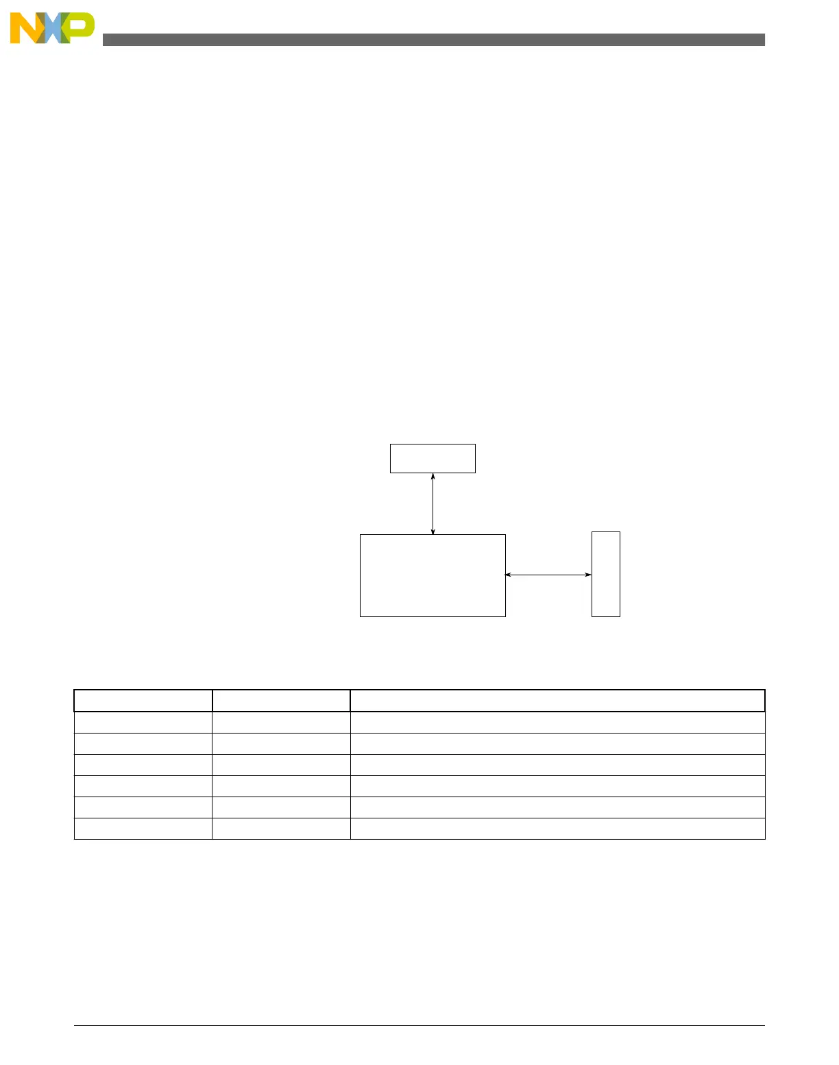
3.9.4 UART Configuration
This section summarizes how the module has been configured in the chip. For a
comprehensive description of the module itself, see the module’s dedicated chapter.
Signal multiplexing
Register
access
Peripheral
bridge
Module signals
UART
Figure 3-36. UART configuration
Table 3-47. Reference links to related information
Topic Related module Reference
Full description UART1 and UART2 UART
Full description UART0 UART
System memory map System memory map
Clocking Clock Distribution
Power management Power management
Signal Multiplexing Port control Signal Multiplexing
Communication interfaces
KL25 Sub-Family Reference Manual, Rev. 3, September 2012
98 Freescale Semiconductor, Inc.

 Loading...


