J: Using a Cascade Summit-12000 Prober Model 4200A-SCS Parameter Analyzer Reference M
J-10 4200A-901-01 Rev. C / February 2017
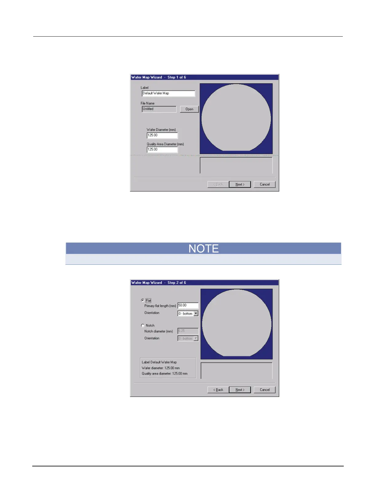
4. From the File menu of the Wafer Map window, select Wizard to start the Wafer Map wizard.
Figure 751: Step 1: Wafer Map Wizard
5. Enter the label and wafer diameter in the Wafer Map Wizard window.
6. Click Next.
7. Select Flat or Notch based on the actual wafer.
8. Enter either the primary flat length or the notch diameter in millimeters.
9. Select the orientation of the flat or notch as applicable.
Bottom is toward the front of the prober.
Figure 752: Step 2: Wafer Map Wizard
10. Click Next.
 Loading...