-SCS Parameter Analyzer Reference Manual Appendix D: Using a Model 82 C-
4200A-901-01 Rev. C / February 2017 D-63
Symbol Description Units
Effective oxide charge concentration.
N(90% W
MAX
)
Doping corresponding to 90% maximum w profile (approximates doping in the
bulk).
1 / cm
Mobile ion concentration in the oxide.
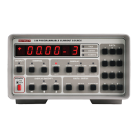
Current measured by the Model 595 at the end of each capacitance
measurement with the unit in the capacitance function.
R
t
Oxide thickness. nm
V
GS
Gate voltage. More specifically, the voltage at the gate with respect to the
Flatband voltage, or the value of V
GS
that results in C
FB
.
V
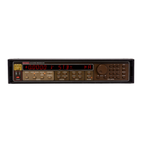
Voltage reading sent by Model 590 with matching C
H
and G.
V
V
TH
The point where the surface potential, ψS, is equal to twice the bulk potential,
φ
V
Depletion depth or thickness. Silicon under the gate is depleted of minority
carriers in inversion and depletion.
ψ
S
Silicon surface potential as a function of V
GS
. More precisely, this value
represents band bending and is related to surface potential via the bulk
V
ψ
Offset in ψS due to calculation method and V
.
φ
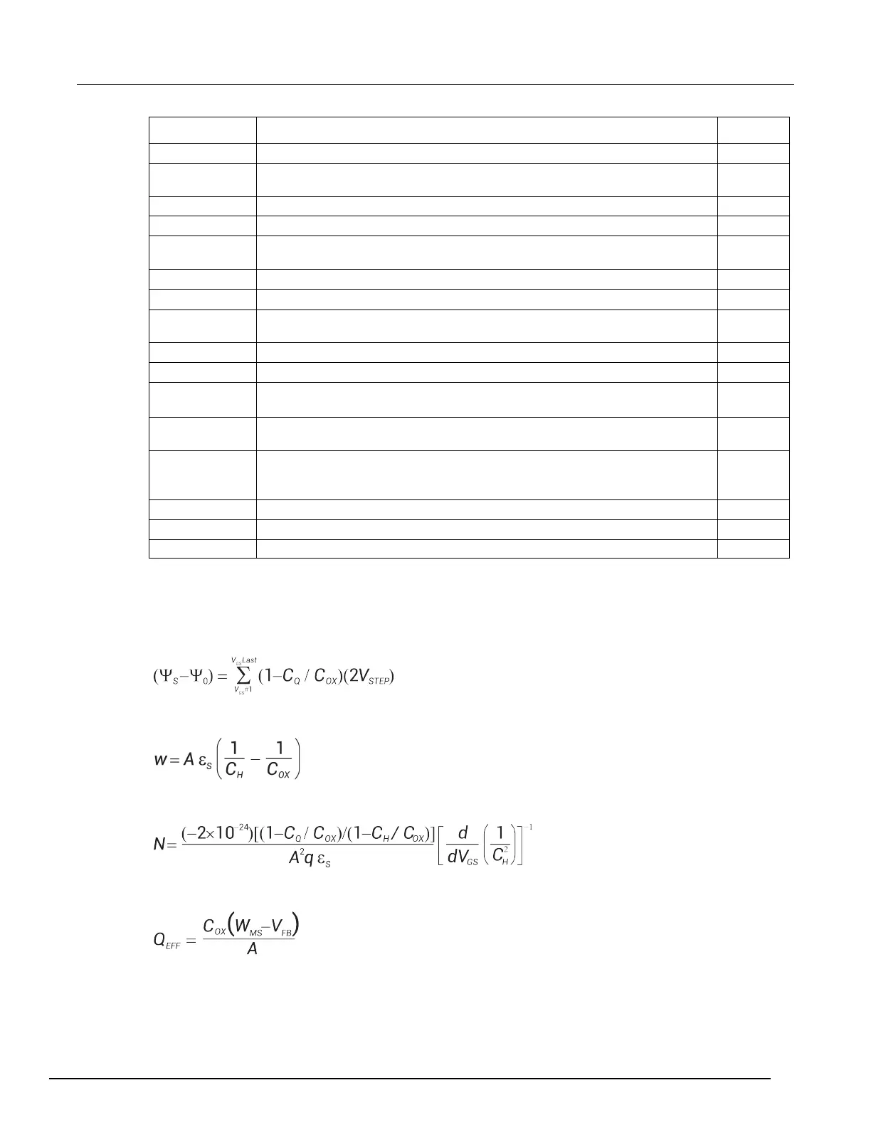
Summary of analysis equations
The analysis equations used by the Model 82 software are summarized in the following.
Band bending
Depletion depth
Doping concentration
Effective oxide charge
 Loading...