L: Wafer-level reliability testing Model 4200A-SCS Parameter Analyzer
L-8 4200A-901-01 Rev. C / February 2017
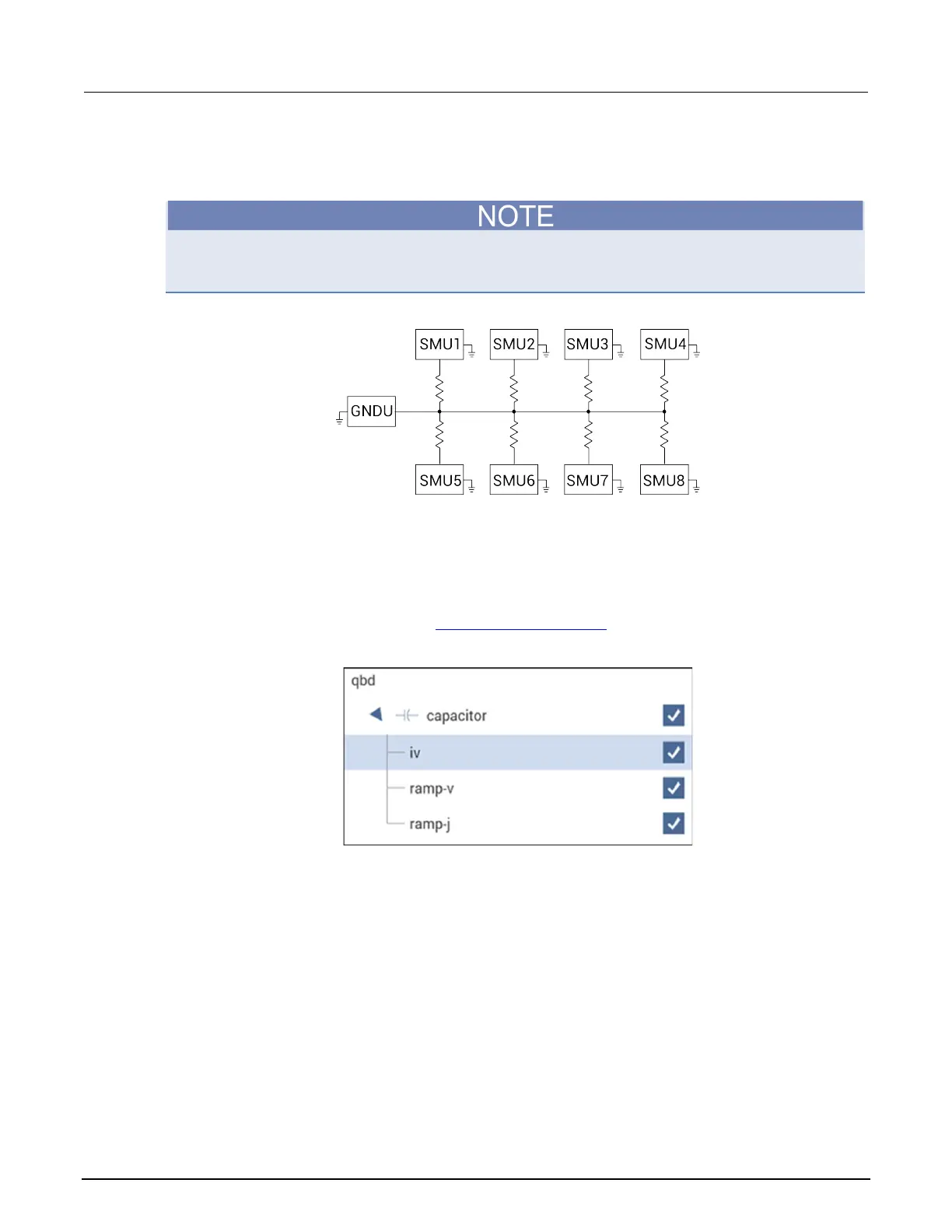
You can modify the em-const-i project to test additional devices. Each SMU in the test system can
current-stress one device. Therefore, if there are eight SMUs in the test system, you can stress up to
eight devices can be stressed, as shown in the following figure.
Current stressing: When setting the current stress level for each device in the subsite, keep in mind
that a setting of zero (0) connects the device pin to the ground unit (0 V ground). In order to current
stress a device, the current stress level must be set to a non-zero value.
Figure 836: EM test: Eight devices being current stressed by eight SMUs
Charge-to-Breakdown Test of Dielectrics project
The qbd project includes tests for the ramp-v test and the ramp-j test. These tests adhere to the
JESD35-A standard procedures for wafer-level testing of thin dielectrics. This project does not use
subsite cycling.
Details on these tests are described in V-ramp and J-ramp tests (on page L-10
).
Figure 837: qbd project tree
 Loading...