4: Multi-frequency capacitance-voltage unit Model 4200A-SCS Parameter Analyzer
4-86 4200A-901-01 Rev. C / February 2017
g-to-sdb and mosfet-dopingprofile Analyze sheet
The test data is displayed in the Analyze sheet:
• Cp_GB: Measured parallel capacitance.
• Gp_GB: Measured conductance.
• DCV_GB: Forced DC bias voltage.
• F_GB: Forced test frequency.
• Formulas: Formulator calculation results.
GB = Gate to bulk.
Nanowire tests
You can use C-V measurements on semiconductor nanowires and nanowire-based devices to derive
important characteristics about the device, including mobility, carrier density, and device speed.
Sometimes the capacitance is plotted as a function of channel length or gate length. These
capacitance measurements can often be quite small, <1 pF. As a result, using proper techniques to
reduce parasitic capacitance from affecting measurement accuracy is important.
These tests perform C-V sweeps on a two-terminal nanowire device. The tests are similar but use
different drive frequencies. The tests generate capacitance versus voltage graphs.
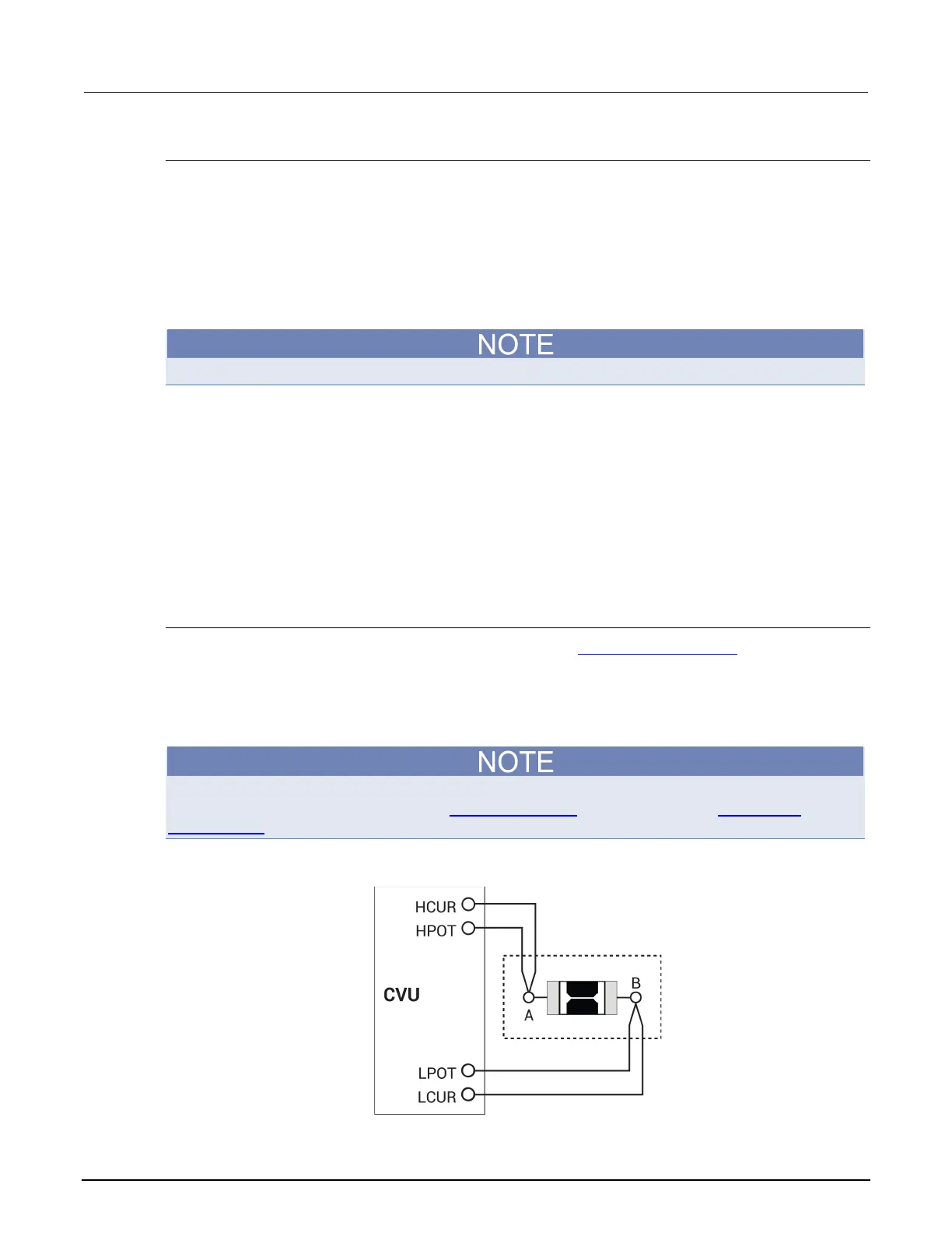
cvu-nanowire connections
The next figure shows the basic test configuration. Refer to 4210-CVU connections (on page 4-5) for
details. The cv-gd test is used to test a nanowire on a wafer. The cv-sd test can be used to test a
nanowire on a wafer or a discrete nanowire device.
Use only the supplied (red) 100 Ω SMA cables for connections to the 4210-CVU. Be sure that all SMA
cables used for the project are the same length.
After making or changing connections, be sure to use the Confidence Check diagnostic tool and do
connection compensation tests. Refer to Confidence Check (on page 4-19) and Connection
compensation (on page 4-10) for details.
Figure 136: Basic configuration to test a nanowire device
 Loading...