K: Using a Signatone CM500 Prober Model 4200A-SCS Parameter Analyzer
K-6 4200A-901-01 Rev. C / February 2017
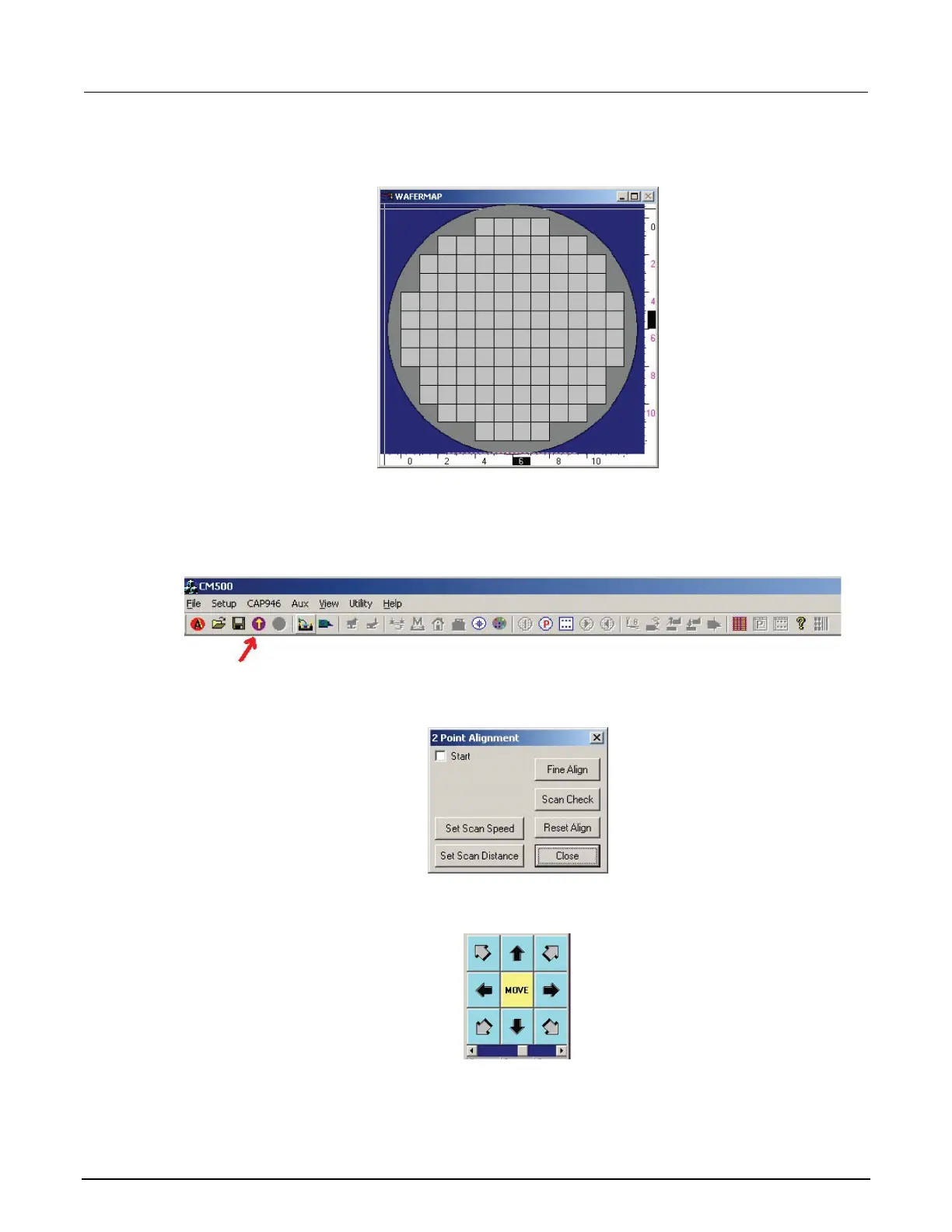
4. After selecting OK, a new wafermap is displayed.
Figure 797: CM500 Prober wafermap
Load, align, and contact the wafer
1. Click the Load wafer icon on toolbar.
Figure 798: CM500 Prober load wafer icon
2. Select Start to move the wafer to Home and begin the sequences of 2-point alignment.
Figure 799: CM500 Prober 2 Point Alignment 1
3. Click the Arrow buttons on the window to move the wafer stage to reference point 1.
Figure 800: CM500 Prober manual MOVE buttons
 Loading...