L: Wafer-level reliability testing Model 4200A-SCS Parameter Analyzer
L-6 4200A-901-01 Rev. C / February 2017
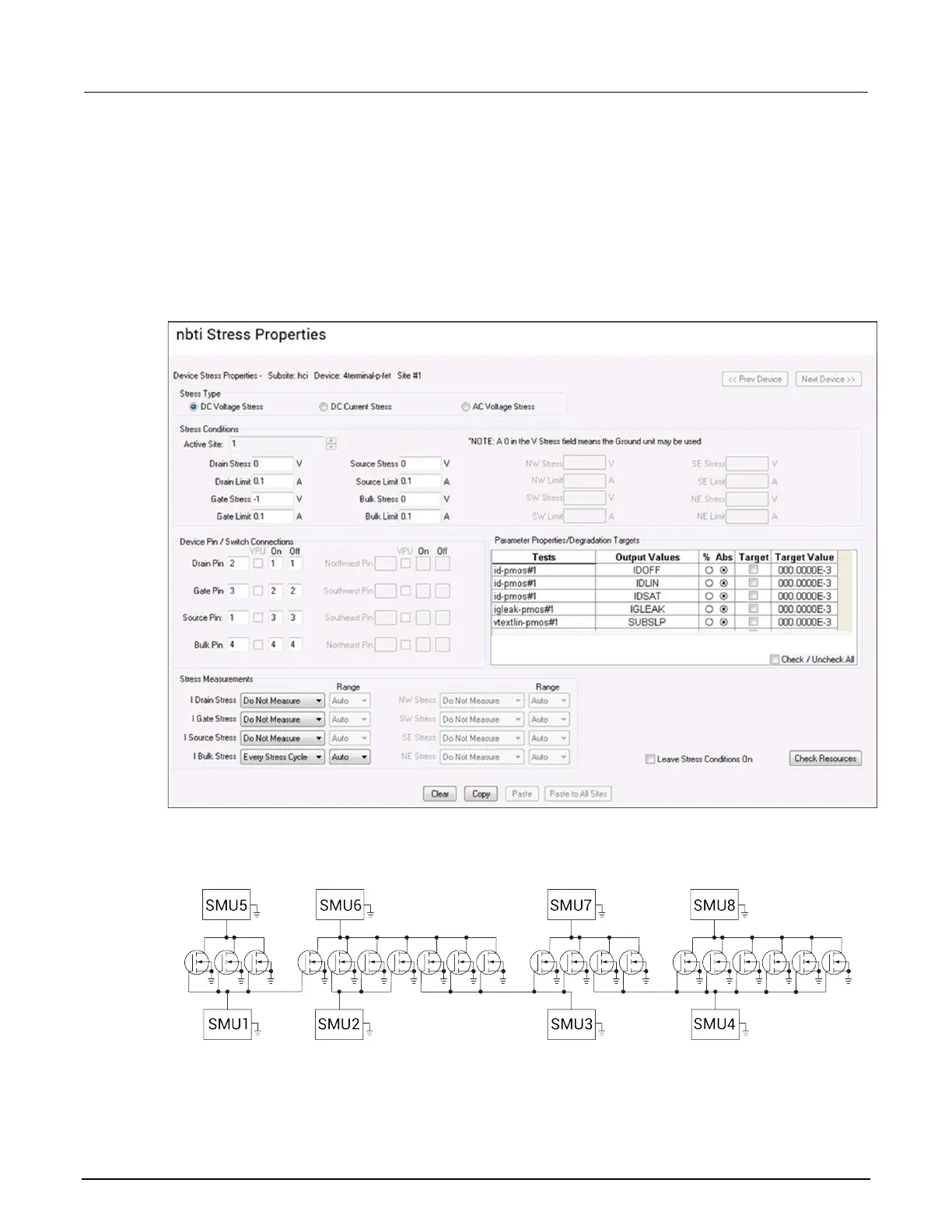
The nbti subsite is configured for subsite cycling using voltage stressing for a p-channel MOSFET
(PMOS) device.
This project includes actions that control the temperature of the chuck. The subsite test will not start
until the chuck reaches the specified temperature. After the first pre-stress cycle to characterize the
device, subsequent cycles voltage stress the device for a specified time before repeating the tests.
After the subsite cycling is complete, the chuck-cooling action cools the chuck.
The Stress Properties Configure pane for the nbti-1-dut project is shown in the following figure.
Figure 832: Stress Properties for the nbti-1-dut project
In a parallel connection scheme, up to 20 devices can be stressed by voltage. The figure below
shows an example of 20 parallel-connected devices being stressed by eight gate and drain voltages.
Figure 833: HCI and NBTI tests: 20 parallel-connected devices stressed by voltage
 Loading...