-SCS Parameter Analyzer Reference Manual Section 4: Multi-frequency capacitance-
4200A-901-01 Rev. C / February 2017 4-45
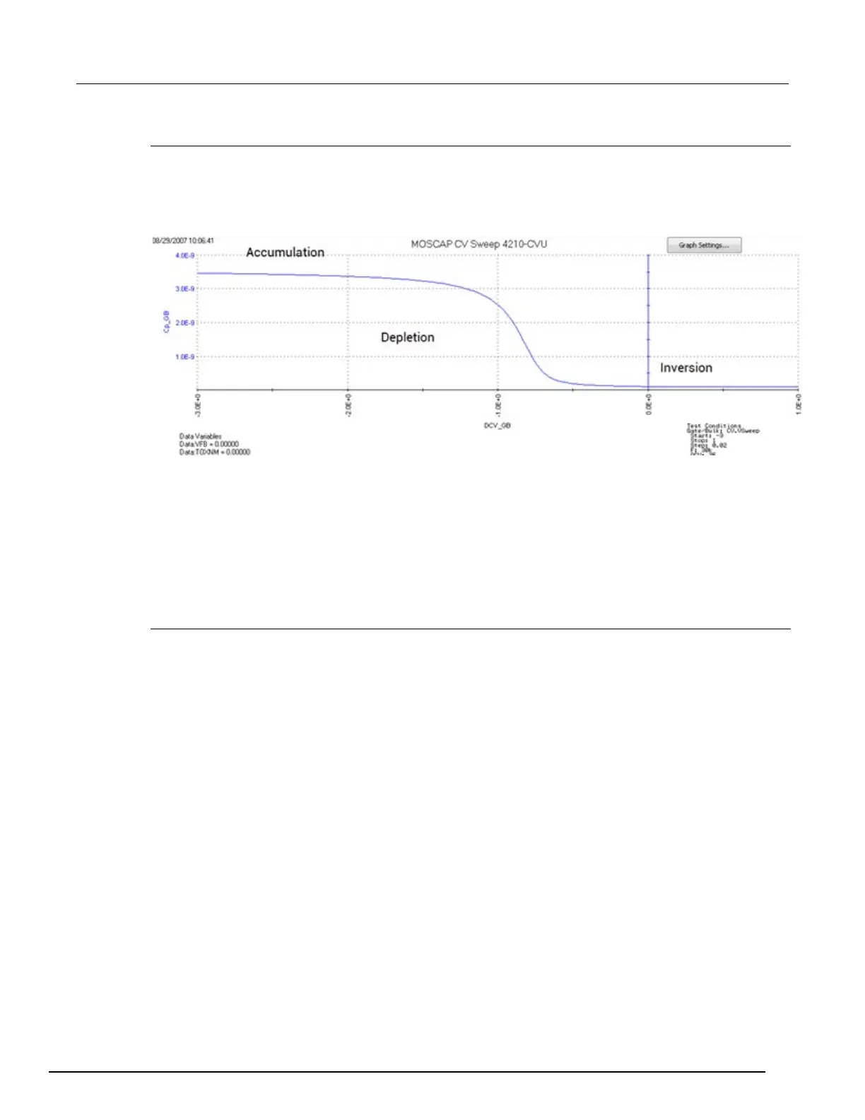
MOS capacitor C-V curves
The next figure illustrates a high-frequency C-V curve for a p-type semiconductor substrate. A C-V
curve can be divided into three regions: accumulation, depletion, and inversion. Each of the three
regions is described for a p-type MOS capacitor.
Figure 124: C-V curve example for p-type MOS-C
The C-V curve for an n-type MOS capacitor is analogous to a p-type, except that:
• The majority carriers are electrons.
• The n-type MOS capacitor curve shape is essentially a mirror image of the p-type MOS capacitor
curve shape.
• The accumulation region occurs at positive polarities.
• The inversion region occurs at negative polarities.
Accumulation region
For a p-type MOS capacitor, the accumulation region of the C-V curve is observed when negative
voltages are applied to the gate. The negative polarity causes majority carriers (holes) to be attracted
toward the gate. Because the oxide is a good insulator, these holes accumulate at the substrate-to-
oxide/well-to-oxide interface.
A C-V test measures the oxide capacitance in the strong accumulation region, where for a p-type
MOS capacitor, the voltage is negative enough that the capacitance is essentially constant and the
C-V curve slope is essentially flat. There, the oxide thickness can be extracted from the oxide
capacitance. However, the C-V curve for a very thin oxide often does not saturate to a flat slope. In
that case, the measured oxide capacitance differs from the true oxide capacitance.
 Loading...