-SCS Parameter Analyzer Reference Manual Section 4: Multi-frequency capacitance-
4200A-901-01 Rev. C / February 2017 4-57
Compensating for series resistance
After generating a C-V curve, you may need to compensate the measurements for series resistance.
The series resistance (R
SERIES
) can be attributed to either the substrate (well) or the backside of the
wafer. For wafers typically produced in fabrication plants, the substrate bulk resistance is small (<10
Ω) and has negligible impact on C-V measurements. However, if the backside of the wafer is used as
an electrical contact, the series resistance due to oxides can significantly distort a measured C-V
curve.
Without series compensation, capacitance can be lower than normal and C-V curves can be
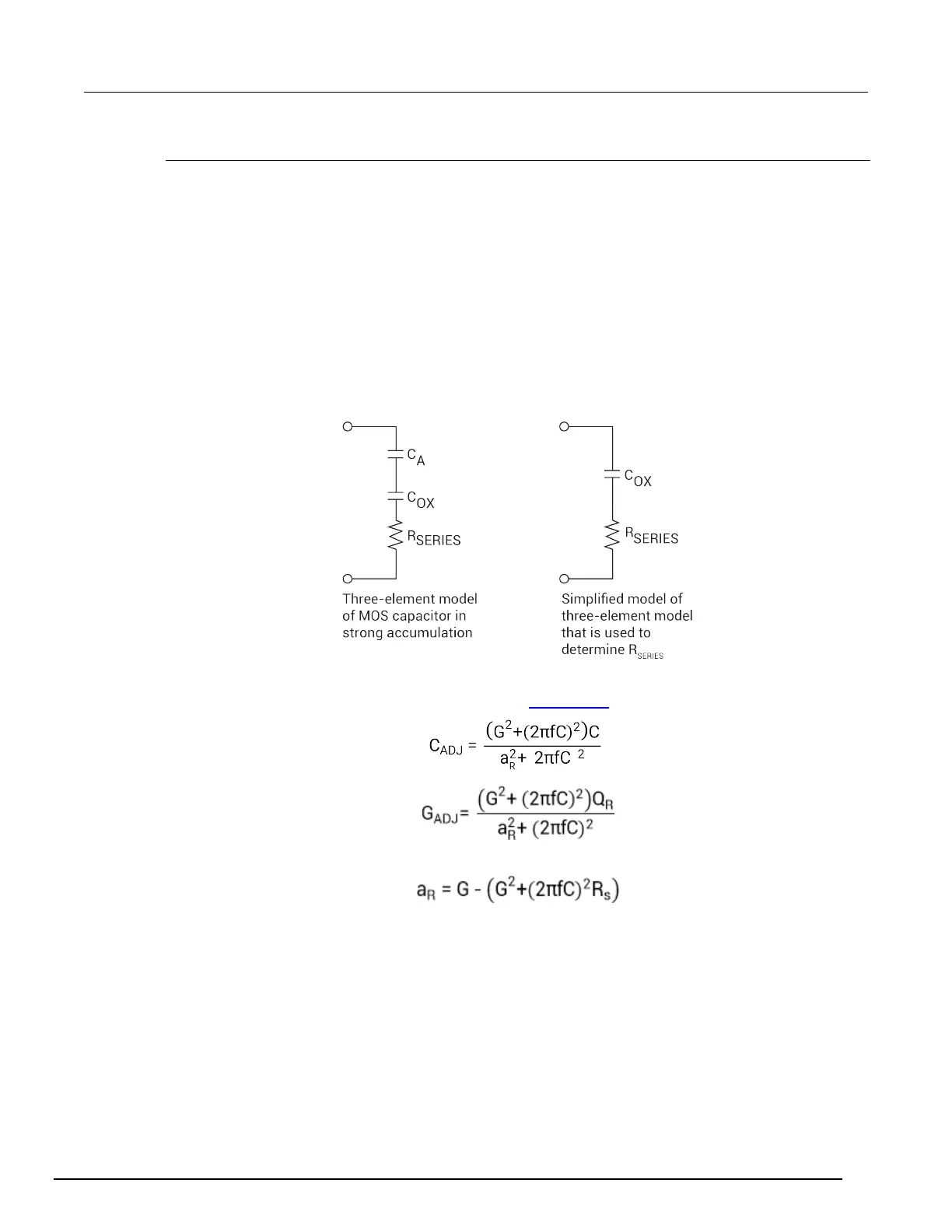
distorted. Tests for this project compensate for series resistance using the simplified 3-element model
shown in the next figure.
In this model, C
OX
is the oxide capacitance while CA is the capacitance of the accumulation layer. The
series resistance is represented by R
SERIES
.
Figure 126: Simplified model to determine series resistance
The corrected capacitance (C
ADJ
) and corrected conductance (G
ADJ
) are calculated from the formulas
shown below (from Nicollian and Brews, p. 224; see References (on page 4-63
)).
Where:
Where:
• C
ADJ
= series resistance compensated parallel model capacitance
• G
ADJ
= series resistance compensated conductance
• C = measured parallel model capacitance
• G = measured conductance
• f = test frequency as set in Clarius
• R
S
= series resistance
 Loading...