-SCS Parameter Analyzer Reference Manual Section 4: Multi-frequency capacitance-
4200A-901-01 Rev. C / February 2017 4-59
Oxide thickness calculations based on C-V measurements can be very precise. Oxide thickness
must be extracted from the strong accumulation region, where the capacitance measured truly
reflects the oxide capacitance.
The oxide capacitance, C
OX
, is set in the Formulator to be the maximum capacitance in accumulation.
Flatband capacitance and flatband voltage
Application of a certain gate voltage, the flatband voltage (V
FB
), results in the disappearance of band
bending. At this point, known as the flatband condition, the semiconductor band is said to become
flat. Because the band is flat, the surface potential is zero, with the reference potential being taken as
the bulk potential deep in the semiconductor. Flatband voltage and its shift are widely used to extract
other device parameters, such as oxide charges.
V
FB
can be identified from the C-V curve. One way is to use the flatband capacitance method. For this
method, the ideal value of the flatband capacitance (C
FB
) is calculated using equations below. Once
the value of C
FB
is known, the value of V
FB
can be obtained from the C-V curve data by interpolating
between the closest gate-to-substrate (V
GS
) values (from Nicollian and Brews pp 487-488; see
References (on page 4-63
)).
The Debye equation calculates the Debye length parameter (λ) that is used in the flatband
capacitance equation. Based on the doping profile, the λ calculation requires one of the following
doping concentrations: N at 90% of W
MAX
(refer to Nicollian and Brews), a user-supplied NA
(bulk-doping concentration for a p-type acceptor material), or a user-supplied ND (bulk doping
concentration for an n-type donor material).
The flatband capacitance method is invalid when the interface trap density (DIT) becomes very large
(10
12
to 10
13
or greater). However, the method should give satisfactory results for most users. Those
dealing with high DIT values should consult the appropriate literature for a more suitable method.
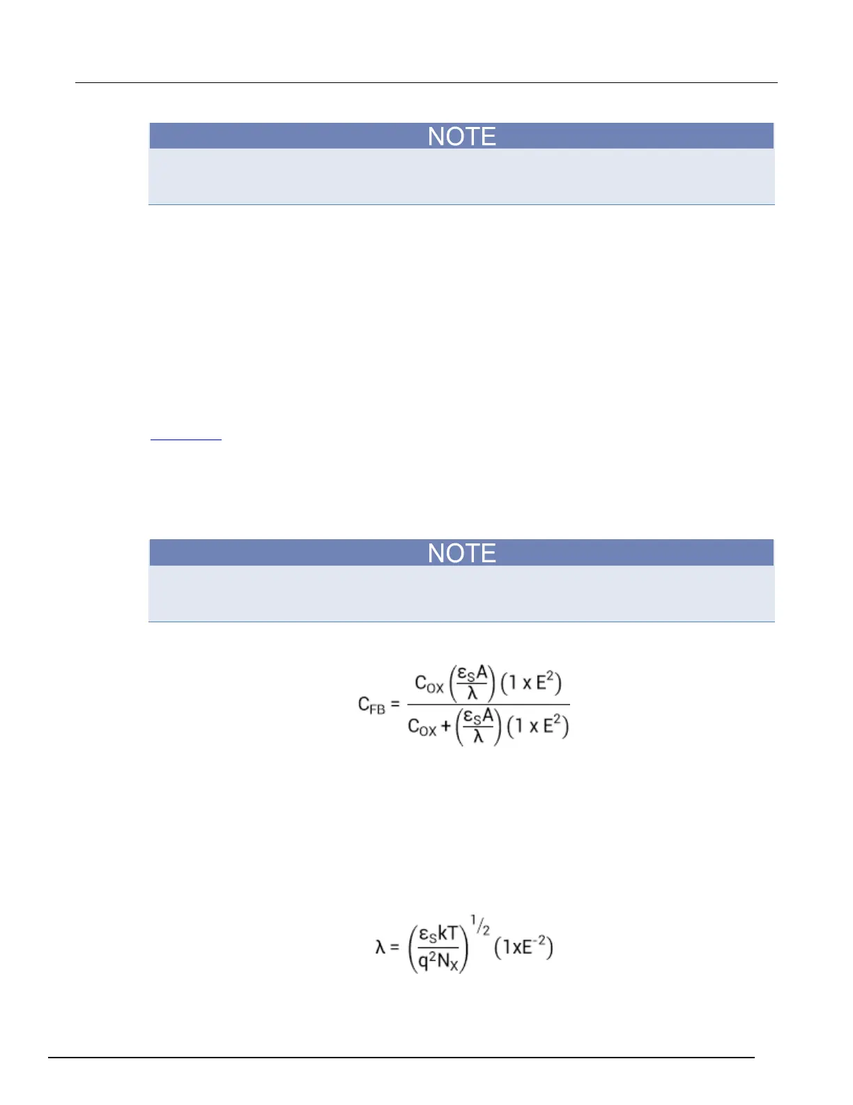
Use the next two equations to calculate the flatband capacitance:
Where:
• CFB = flatband capacitance (F)
• C
ox
= oxide capacitance (F)
• ε
s
= permittivity of the substrate material (F/cm)
• A = gate area (cm
2
)
• 1 x E
2
= units conversion from m to cm
• λ = extrinsic Debye length, which is calculated as follows:
 Loading...