-SCS Parameter Analyzer Reference Manual Section 4: Multi-frequency capacitance-
4200A-901-01 Rev. C / February 2017 4-61
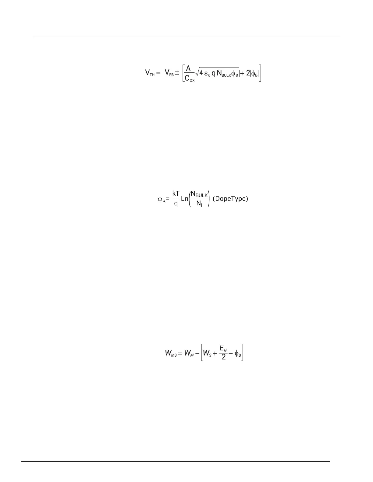
The threshold voltage of a MOS capacitor can be calculated as follows:
Where:
• V
TH
= threshold voltage (V)
• V
FB
= flatband potential (V)
• A = gate area (cm
2
)
• C
OX
= oxide capacitance (F)
• ε
S
= permittivity of substrate material (F/cm)
• q = electron charge (1.60219 x 10
-19
coulombs)
• N
BULK
= bulk doping (cm
-3
); note that the Formulator name for N
BULK
is N90W
• φ
B
= bulk potential (V); note that the Formulator name for φ
B
is PHIB
The bulk potential is calculated as follows:
Where:
• φ
B
= bulk potential (V); note that the Formulator name for φ
B
is PHIB
• k = Boltzmann’s constant (1.3807 x 10
-23
J/K)
• T = Test temperature (K)
• q = electron charge (1.60219 x 10
-19
coulombs)
• N
BULK
= bulk doping (cm
-3
); note that the Formulator name for N
BULK
is N90W
• N
i
= intrinsic carrier concentration (1.45 x 10
10
cm
-3
)
• DopeType = +1 for p-type materials and -1 for n-type materials; note that the value for DopeType
is changed in the Constants area of the Formulator
Metal semiconductor work function difference
The metal semiconductor work function difference, W
MS
, is commonly referred to as the work function.
It contributes to the shift in V
FB
from the ideal zero value, along with the effective oxide charge
(Nicollian and Brews 462-477; Sze 395402). The work function represents the difference in work
necessary to remove an electron from the gate and from the substrate, and it is derived as follows:
 Loading...