Chapter 14
390 MIPS R4000 Microprocessor User's Manual
14.1 What Boundary Scanning Is
With the evolution of ever-denser integrated circuits (ICs), surface-
mounted devices, double-sided component mounting on printed-circuit
boards (PCBs), and buried vias, in-circuit tests that depend upon making
physical contact with internal board and chip connections have become
more and more difficult to use. The greater complexity of ICs has also
meant that tests to fully exercise these chips have become much larger and
more difficult to write.
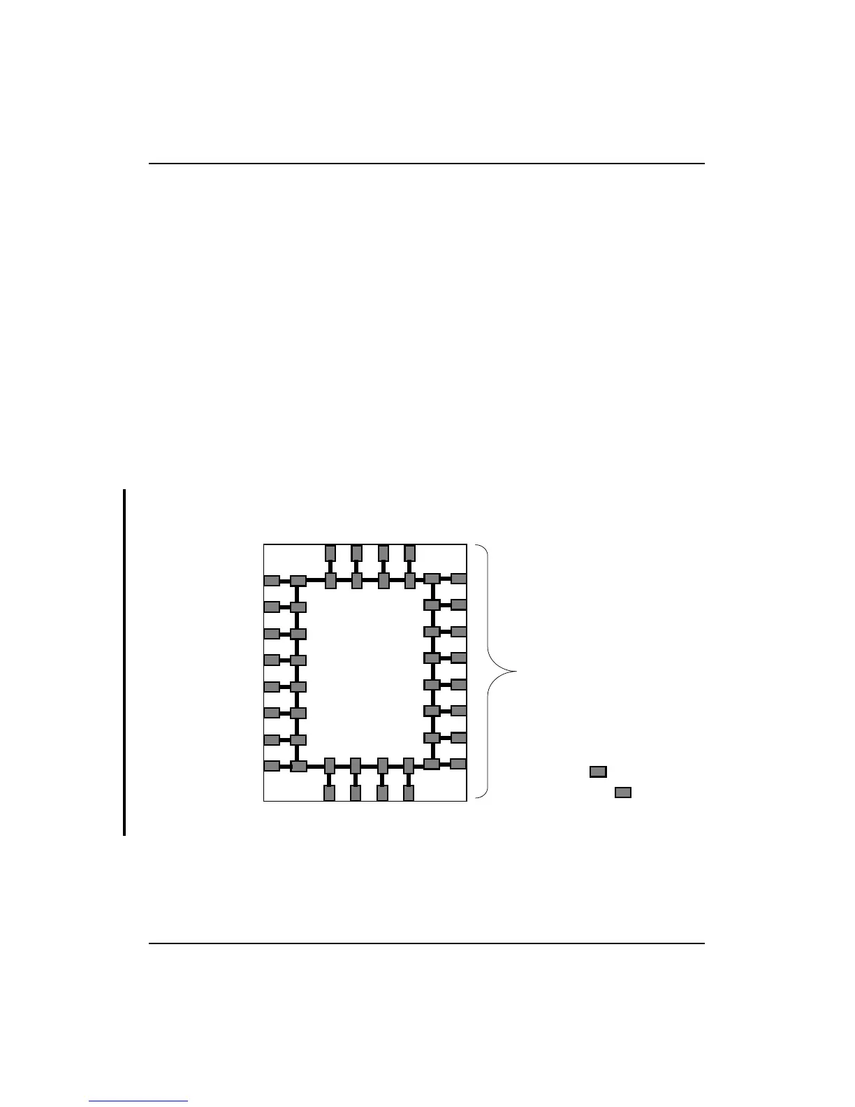
One solution to this difficulty has been the development of boundary-scan
circuits. A boundary-scan circuit is a series of shift register cells placed
between each pin and the internal circuitry of the IC to which the pin is
connected, as shown in Figure 14-1. Normally, these boundary-scan cells
are bypassed; when the IC enters test mode, however, the scan cells can be
directed by the test program to pass data along the shift register path and
perform various diagnostic tests. To accomplish this, the tests use the four
signals described in the next section: JTDI, JTDO, JTMS, and JTCK.
Figure 14-1 JTAG Boundary-scan Cells
Boundary-scan cells
IC package pin
Integrated
Circuit