MIPS R4000 Microprocessor User's Manual 93
Memory Management
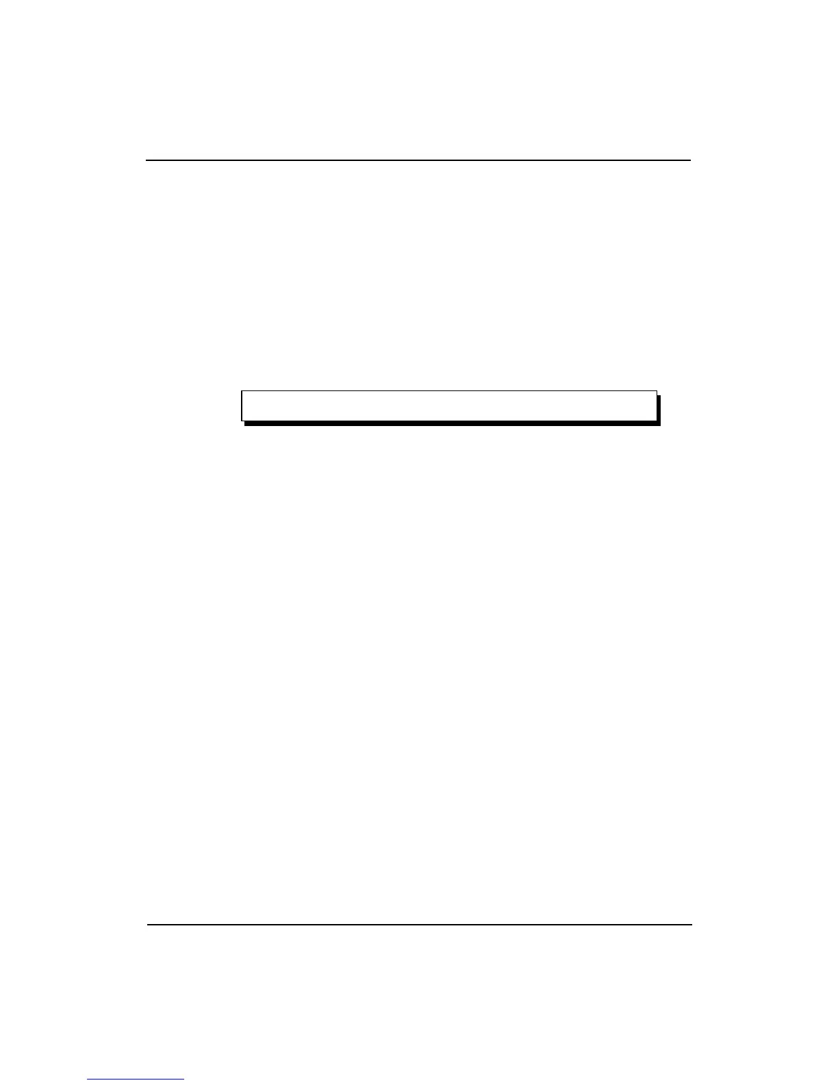
Load Linked Address (LLAddr) Register (17)
The read/write Load Linked Address (LLAddr) register contains the physical
address read by the most recent Load Linked instruction.
This register is for diagnostic purposes only, and serves no function
during normal operation.
Figure 4-17 shows the format of the LLAddr register; PAddr represents bits
of the physical address, PA(35:4).
Figure 4-17 LLAddr Register Format
Cache Tag Registers [TagLo (28) and TagHi (29)]
The TagLo and TagHi registers are 32-bit read/write registers that hold
either the primary cache tag and parity, or the secondary cache tag and
ECC during cache initialization, cache diagnostics, or cache error
processing. The Tag registers are written by the CACHE and MTC0
instructions.
The P and ECC fields of these registers are ignored on Index Store Tag
operations. Parity and ECC are computed by the store operation.
Figure 4-18 shows the format of these registers for primary cache
operations. Figure 4-19 shows the format of these registers for secondary
cache operations.
Table 4-13 lists the field definitions of the TagLo and TagHi registers.
LLAddr Register
31 0
PAddr(35:4)
32