MIPS R4000 Microprocessor User's Manual 395
JTAG Interface
Test Access Port (TAP)
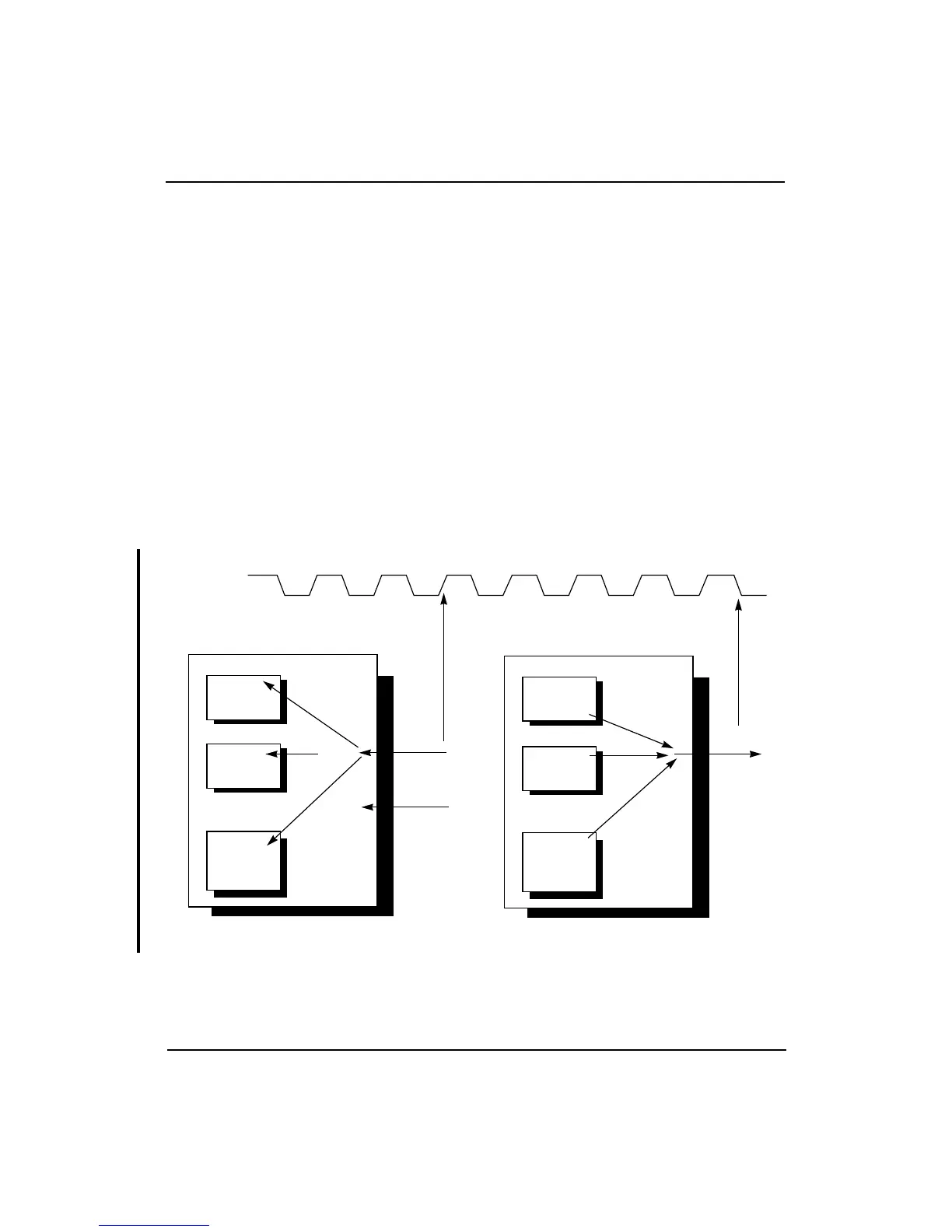
The Test Access Port (TAP) consists of the four signal pins: JTDI, JTDO,
JTMS, and JTCK. Serial test data and instructions are communicated
over these four signal pins, along with control of the test to be executed.
As Figure 14-6 shows, data is serially scanned into one of the three
registers (Instruction register, Bypass register, or the Boundary-scan register)
from the JTDI pin, or it is scanned from one of these three registers onto
the JTDO pin.
The JTDI input feeds the least-significant bit (LSB) of the selected register,
whereas the most-significant bit (MSB) of the selected register appears on
the JTDO output.
The JTMS input controls the state transitions of the main TAP controller
state machine.
The JTCK input is a dedicated test clock that allows serial JTAG data to be
shifted synchronously, independent of any chip-specific or system clocks.
Figure 14-6 JTAG Test Access Port
Data on the JTDI and JTMS pins is sampled on the rising edge of the
JTCK input clock signal. Data on the JTDO pin changes on the falling
edge of the JTCK clock signal.
JTD0 pin
CPU
Data scanned in serially
Context is
saved
Instruction
register
Context is
saved
Boundary-
scan
register
Context is
saved
Bypass
register
Data scanned out serially
02
0
1
319
CPU
Context is
saved
Instruction
register
Context is
saved
Boundary-
scan
register
Context is
saved
Bypass
register
02
0
1
319
LSB
(MSB)
JTDI pin
JTMS pin
JTMS and JTDI sampled
on rising edge of JTCK
JTCK
JTD0 sampled on
falling edge of JTCK