MIPS R4000 Microprocessor User's Manual 393
JTAG Interface
Bypass Register
The Bypass register is 1 bit wide. When the TAP controller is in the Shift-
DR (Bypass) state, the data on the JTDI pin is shifted into the Bypass
register, and the Bypass register output shifts to the JTDO output pin.
In essence, the Bypass register is a short-circuit which allows bypassing of
board-level devices, in the serial boundary-scan chain, which are not
required for a specific test. The logical location of the Bypass register in the
boundary-scan chain is shown in Figure 14-4. Use of the Bypass register
speeds up access to boundary-scan registers in those ICs that remain
active in the board-level test datapath.
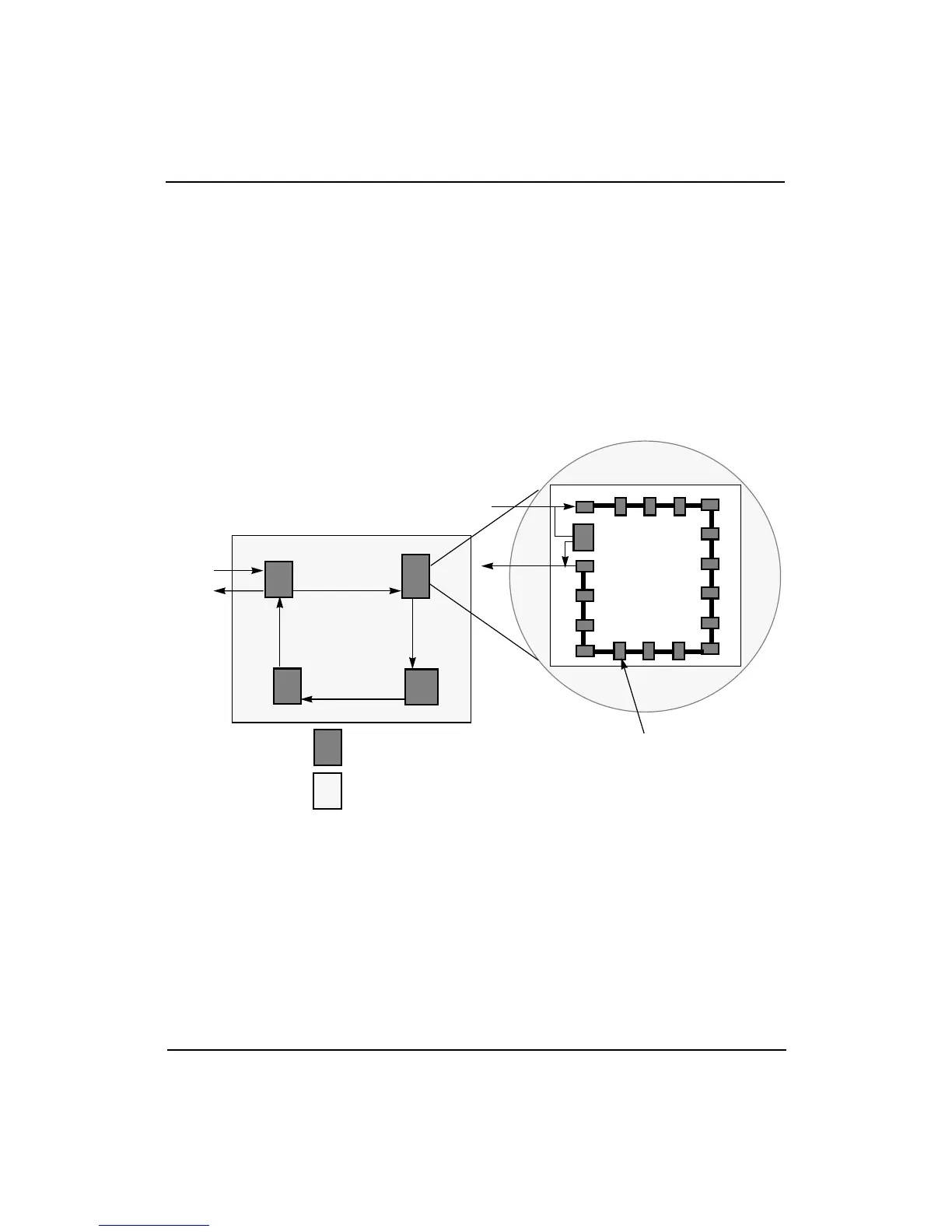
Figure 14-4 Bypass Register Operation
Board
IC package
JTDO
Bypass
register
JTDI
JTDO
JTDI
JTDO
JTDI
JTDO
JTDI
Board
input
Board
output
JTDI
JTDO
Boundary-scan
register pad cell