MIPS R4000 Microprocessor User's Manual 205
R4000 Processor Signal Descriptions
8.3 Secondary Cache Interface Signals
Secondary Cache interface signals constitute the interface between the
R4000 processor and secondary cache. These signals are available only on
the R4000MC and R4000SC. Table 8-3 lists the Secondary Cache interface
signals.
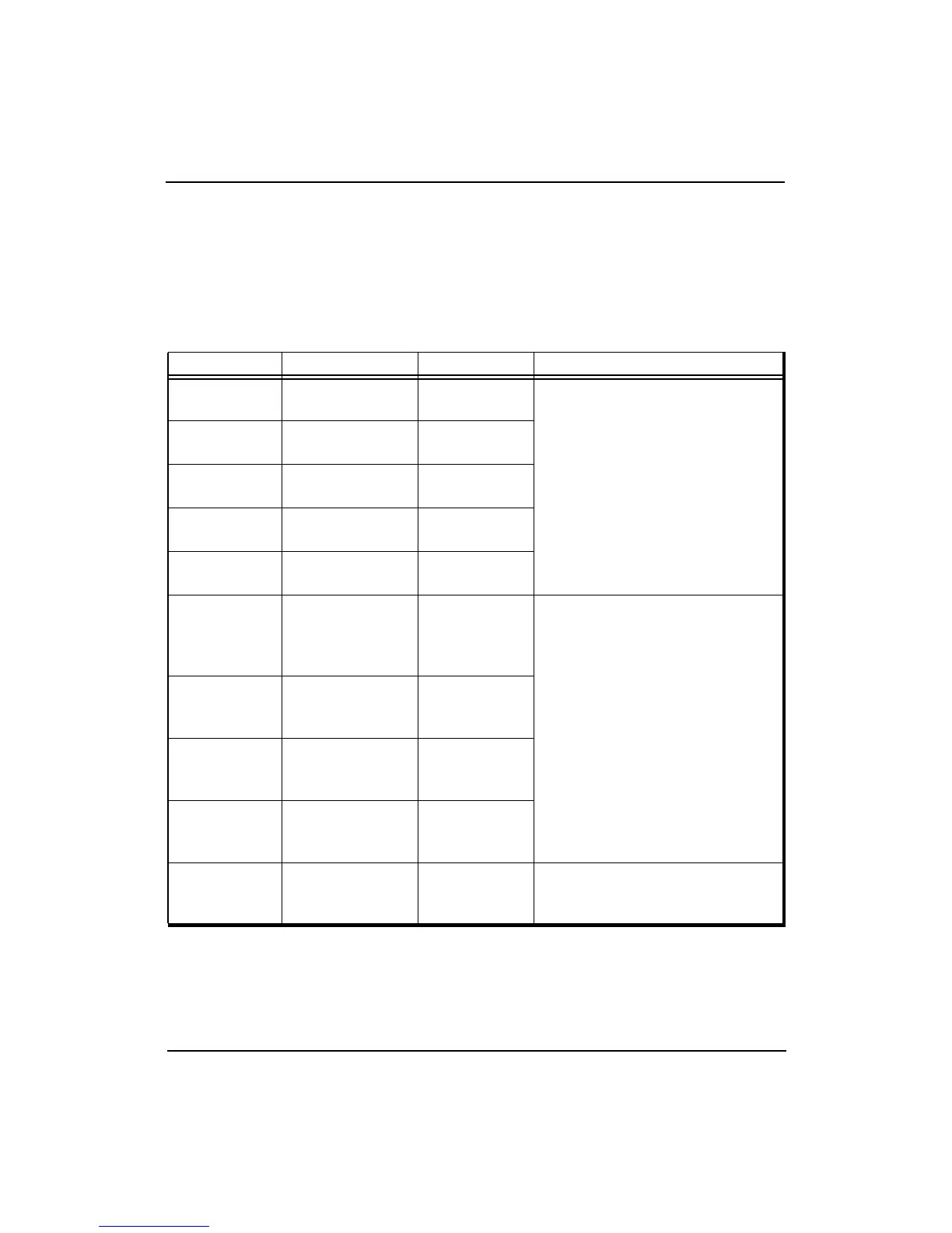
Table 8-3 Secondary Cache Interface Signals
Name Definition Direction Description
SCAddr(17:1)
Secondary cache
address bus
Output
The 18-bit address bus for the
secondary cache. Bit 0 has four
output lines, (SCAddr0W:Z), to
provide additional drive current.
SCAddr0W
Secondary cache
address LSB
Output
SCAddr0X
Secondary cache
address LSB
Output
SCAddr0Y
Secondary cache
address LSB
Output
SCAddr0Z
Secondary cache
address LSB
Output
SCAPar(2:0)
Secondary cache
address parity
bus
Output
A 3-bit bus that carries the parity
of the SCAddr bus and the cache
control line SCWr*. The
individual bit definitions are:
SCAPar2
Secondary cache
address parity
bus
Output
Even parity for SCAddr(17:12)
and SCWr*
SCAPar1
Secondary cache
address parity
bus
Output
Even parity for SCAddr(11:6) and
SCDCS*
SCAPar0
Secondary cache
address parity
bus
Output
Even parity for SCAddr(5:0) and
SCTCS*
SCData(127:0)
Secondary cache
data bus
Input/Output
A 128-bit bus used to read or write
cache data from and to the
secondary cache data RAM.