D: Using a Model 82 C-V System Model 4200A-SCS Parameter Analyzer
D-50 4200A-901-01 Rev. C / February 2017
Gain and offset
Gain and offset can be applied to C
Q
and C
H
data to allow for curve alignment or to compensate for
measurement errors. A gain factor is a multiplier that is applied to all elements of C
Q
or C
H
array data
before plotting or graphics array calculation. Offset is a constant value added to or subtracted from all
C
Q
and C
H
data before plotting or array calculation.
For example, assume that you compare the C
Q
and Cn values at reading #3, and you find that C
Q
is
2.3 pF less than Cn. If you then add an offset of +2.3 pF to C
Q
, the C
Q
and C
H
values at reading #3
will then be the same, and the C
Q
and C
H
curves will be aligned at that point.
Gain and offset values do not affect raw C
Q
and C
H
values stored in the data file, but the gain and
offset values are stored in the data file so compensated curves can be easily regenerated at a later
date.
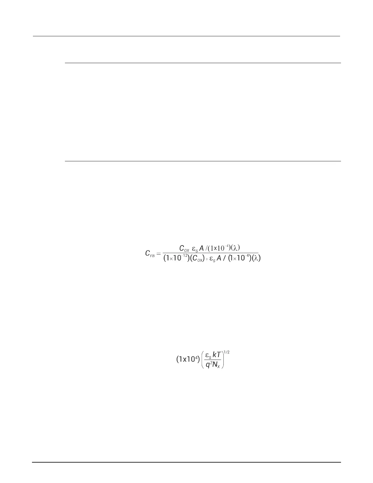
Flatband capacitance and flatband voltage
The Model 82 uses the flatband capacitance method of finding flatband voltage, V
FB
. The Debye
length is used to calculate the ideal value of flatband capacitance, C
FB
. Once the value of C
FB
is
known, the value of V
FB
is interpolated from the closest V
G
values (Nicollian and Brews 487-488).
The method used is invalid when interface trap density becomes very large (1012-1013 and greater).
However, this algorithm should give satisfactory results for most users. Those who are dealing with
high values of D
IT
should consult the appropriate literature for a more appropriate method.
Based on doping, the calculation of C
FB
uses N at 90% W
MAX
, or user-supplied N
A
(bulk doping for p-
type, acceptors) or N
D
(bulk doping for n-type, donors).
C
FB
is calculated as follows:
Where:
• C
FB
= flatband capacitance (pF)
• C
OX
= oxide capacitance (pF)
• ε
S
= permittivity of substrate material (F/cm)
• A = gate area (cm
2
)
• 1 × 10
-4
= units conversion for λ
• 1 × 10
-12
= units conversion for C
OX
And λ = extrinsic Debye length =
Where:
• kT = thermal energy at room temperature (4,046 × 10
-21
J)
• q = electron charge (1.60219 × 10
-19
coulombs)
• N
x
= N at 90% W
MAX
, or N
A
, or N
D
when input by the user
• N at 90% W
MAX
is chosen to represent bulk doping
 Loading...