-SCS Parameter Analyzer Reference Manual Section 4: Multi-frequency capacitance-voltag
4200A-901-01 Rev. C / February 2017 4-89
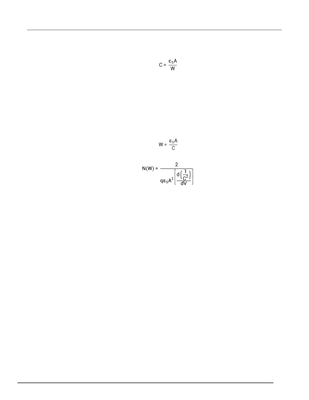
Since the junction can be modeled after a parallel plate capacitor, the junction capacitance is
calculated as follows:
Where:
• C = junction capacitance (F)
• εs = semiconductor permittivity (1.034e-12 F/cm for silicon)
• A = area of junction (cm
2
)
• W = depletion width (cm)
However, unlike the parallel plate capacitor, the depletion layer width (W) is not a constant, but is
dependent on the applied voltage. From the previous equation the depletion depth, W, can be
calculated as follows:
From the measured capacitance and the voltage, the doping density can be calculated as follows:
Where:
• N(W) = doping density (cm
-3
)
• A = area of junction (cm
2
)
• C = junction capacitance (F)
• εs = semiconductor permittivity (1.034e-12 F/cm for silicon)
• q = electron charge (1.60219e-19 C)
• V = junction voltage
 Loading...