Table 3-32. Number of KL25 ADC channels (continued)
Device Number of ADC channels
MKL25Z64VLK4 14
MKL25Z128VLK4 14
3.7.1.2 DMA Support on ADC
Applications may require continuous sampling of the ADC that may have considerable
load on the CPU. The ADC supports DMA request functionality for higher performance
when the ADC is sampled at a very high rate. The ADC can trigger the DMA (via DMA
req) on conversion completion.
3.7.1.3 ADC0 Connections/Channel Assignment
NOTE
As indicated by the following sections, each ADCx_DPx input
and certain ADCx_DMx inputs may operate as single-ended
ADC channels in single-ended mode.
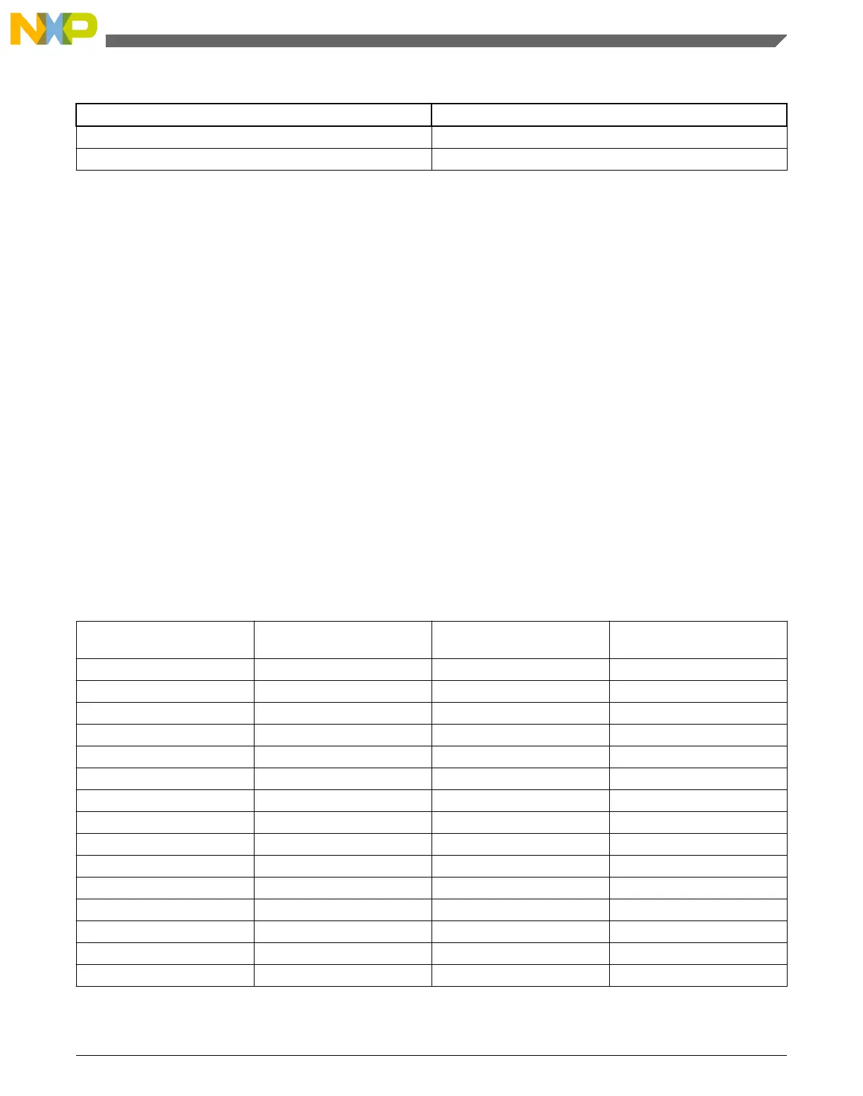
3.7.1.3.1 ADC0 Channel Assignment
ADC Channel
(SC1n[ADCH])
Channel Input signal
(SC1n[DIFF]= 1)
Input signal
(SC1n[DIFF]= 0)
00000 DAD0 ADC0_DP0 and ADC0_DM0 ADC0_DP0/ADC0_SE0
00001 DAD1 ADC0_DP1 and ADC0_DM1 ADC0_DP1/ADC0_SE1
00010 DAD2 ADC0_DP2 and ADC0_DM2 ADC0_DP2/ADC0_SE2
00011 DAD3 ADC0_DP3 and ADC0_DM3 ADC0_DP3/ADC0_SE3
00100
1
AD4a Reserved ADC0_DM0/ADC0_SE4a
00101
1
AD5a Reserved ADC0_DM1/ADC0_SE5a
00110
1
AD6a Reserved ADC0_DM2/ADC0_SE6a
00111
1
AD7a Reserved ADC0_DM3/ADC0_SE7a
00100
1
AD4b Reserved ADC0_SE4b
00101
1
AD5b Reserved ADC0_SE5b
00110
1
AD6b Reserved ADC0_SE6b
00111
1
AD7b Reserved ADC0_SE7b
01000 AD8 Reserved ADC0_SE8
01001 AD9 Reserved ADC0_SE9
01010 AD10 Reserved Reserved
Table continues on the next page...
Chapter 3 Chip Configuration
KL25 Sub-Family Reference Manual, Rev. 3, September 2012
Freescale Semiconductor, Inc. 79

 Loading...


