DocID13284 Rev 2 141/564
UM0404 Parallel ports
With the end of reset, the selected bus configuration will be written to the BUSCON0
register. The configuration of the high byte of PORT0, will be copied into the special register
RP0H.
This read-only register holds the selection for the number of chip selects and segment
addresses. Software can read this register in order to react according to the selected
configuration, if required. When the reset is terminated, the internal pull-up devices are
switched off, and PORT0 will be switched to the appropriate operating mode.
During external accesses in multiplexed bus modes PORT0 first outputs the 16-bit intra-
segment address as an alternate output function. PORT0 is then switched to high-
impedance input mode to read the incoming instruction or data.
In 8-bit data bus mode, two memory cycles are required for word accesses, the first for the
low byte and the second for the high byte of the word. During write cycles PORT0 outputs
the data byte or word after outputting the address. During external accesses in de-
multiplexed bus modes PORT0 reads the incoming instruction or data word or outputs the
data byte or word (see Figure 28).
When an external bus mode is enabled, the direction of the port pin and the loading of data
into the port output latch are controlled by the bus controller hardware. The input of the port
output latch is disconnected from the internal bus and is switched to the line labeled
“Alternate Data Output” via a multiplexer. The alternate data can be the 16-bit intra-segment
address or the 8/16-bit data information. The incoming data on PORT0 is read on the line
“Alternate Data Input”. While an external bus mode is enabled, the user software should not
write to the port output latch, otherwise unpredictable results may occur. When the external
bus modes are disabled, the contents of the direction register last written by the user
becomes active.
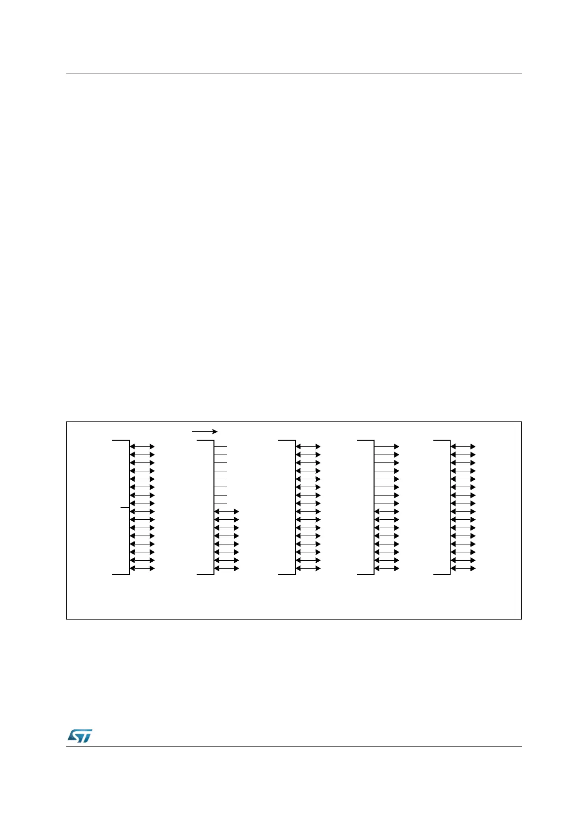
Figure 28. PORT0 I/O and alternate functions
The Figure 29 shows the structure of a PORT0 pin.
PORT0
P0H
P0L
Alternate Functions a) b) c) d)
General
Purpose
8-bit
De-multiplexed
16-bit
De-multiplexed
Bus
8-bit
Multiplexed
Bus
16-bit
Multiplexed
Bus
D7
D6
D5
D4
D3
D2
D1
D0
P0L.7
P0L.6
P0L.5
P0L.4
P0L.3
P0L.2
P0L.1
P0L.0
P0H.7
P0H.6
P0H.5
P0H.4
P0H.3
P0H.2
P0H.1
P0H.0
D7
D6
D5
D4
D3
D2
D1
D0
D15
D14
D13
D12
D11
D10
D9
D8
AD7
AD6
AD5
AD4
AD3
AD2
AD1
AD0
A15
A14
A13
A12
A11
A10
A9
A8
AD7
AD6
AD5
AD4
AD3
AD2
AD1
AD0
AD15
AD14
AD13
AD12
AD11
AD10
AD9
AD8