System reset UM0404
474/564 DocID13284 Rev 2
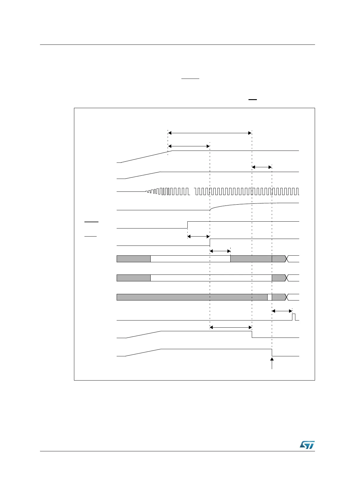
Figure 192 and Figure 193 show Asynchronous Power-On timing diagrams, respectively
with boot from internal or external memory, highlighting the reset phase extension
introduced by the embedded Flash module when selected.
Note: Never power the device without keeping RSTIN
pin grounded: the device could enter in
unpredictable states, risking also permanent damages.
Figure 192. Asynchronous power-on RESET (EA
= 1)
RSTF
P0[15:13]
P0[12:2]
transparent
transparent
P0[1:0] not t.
not transparent
FLARST
V
18
XTAL1
...
≤
2 TCL
RST
≤ 1 ms
Latching point of Port0 for
system start-up configuration
V
DD
≥ 1 ms (for on-chip VREG stabilization)
RPD
IBUS-CS
≤ 1.2 ms (for resonator oscillation + PLL stabilization)
≤ 10.2 ms (for crystal oscillation + PLL stabilization)
RSTIN
(After Filter)
≤ 500 ns
≥ 50 ns
7 TCL
3..4 TCL
(Internal)
not t.
not t.
not t.