The capture / compare units UM0404
338/564 DocID13284 Rev 2
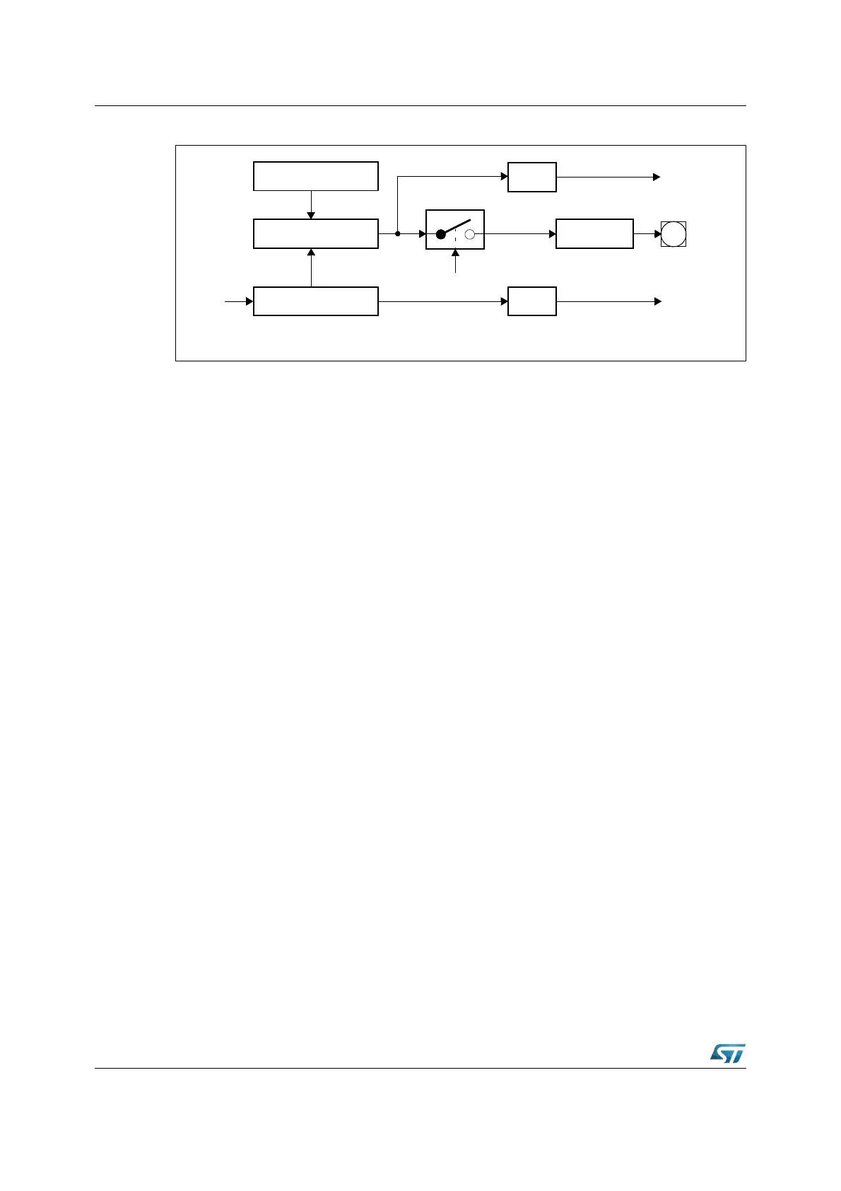
Figure 138. Compare mode 0 and 1 block diagram
Note: The port latch and pin remain unaffected in compare mode 0.
In the example below, the compare value in register CCx is modified from cv1 to cv2 after
compare events #1 and #3, and from cv2 to cv1 after events #2 and #4, etc. This results in
periodic interrupt requests from timer Ty, and in interrupt requests from register CCx which
occur at the time specified by the user through cv1 and cv2 (see Figure 139).
16.5.2 Compare mode 1
Compare mode 1 is selected for register CCx by setting bit-field CCMODx of the
corresponding mode control register to ‘101b’.
When a match between the content of the allocated timer and the compare value in register
CCx is detected in this mode, interrupt request flag CCxIR is set to ‘1’, and in addition the
corresponding output pin CCxIO (alternate port output function) is toggled. For this purpose,
the state of the respective port output latch (not the pin) is read, inverted, and then written
back to the output latch.
Compare mode 1 allows several compare events within a single timer period. An overflow of
the allocated timer has no effect on the output pin, nor does it disable or enable further
compare events.
In order to use the respective port pin as compare signal output pin CCxIO for compare
register CCx in compare mode 1, this port pin must be configured as output, and the
corresponding direction control bit must be set to ‘1’. With this configuration, the initial state
of the output signal can be programmed or its state can be modified at any time by writing to
the port output latch.
In compare mode 1 the port latch is toggled upon each compare event (see Figure 139).
Note: If the port output latch is written to by software at the same time it would be altered by a
compare event, the software write will have priority. In this case the hardware-triggered
change will not become effective.
If compare mode 1 is programmed for one of the registers CC0...CC7 or CC16...CC23 the
double-register compare mode becomes enabled for this register if the corresponding bank
1 register is programmed to compare mode 0 (see section Section 16.5.5: Double register
compare mode).
Note: If the port output latch is written to by software at the same time it would be altered by a
compare event, the software write will have priority. In this case the hardware-triggered
change will not become effective.
Capture Register CCx
CAPCOM Timer Ty
TyIR
Interrupt
Request
Input
Clock
x = 31...0
y = 0, 1, 7, 8
CCxIR
Comparator
CCMODx
Port Latch
Toggle
(Mode 1)
CCxIO
Interrupt
Request