The capture / compare units UM0404
342/564 DocID13284 Rev 2
The double-register compare mode can be programmed individually for each register pair.
In order to enable double-register mode the respective bank 1 register (see Table 50) must
be programmed to compare mode 1 and the corresponding bank 2 register (see Table 50)
must be programmed to compare mode 0.
If the respective bank 1 compare register is disabled or programmed for a mode other than
mode 1 the corresponding bank 2 register will operate in compare mode 0 (interrupt-only
mode).
In the following, a bank 2 register (programmed to compare mode 0) will be referred to as
CCz while the corresponding bank 1 register (programmed to compare mode 1) will be
referred to as CCx.
When a match is detected for one of the two registers in a register pair (CCx or CCz) the
associated interrupt request flag (CCxIR or CCzIR) is set to ‘1’ and pin CCxIO
corresponding to bank 1 register CCx is toggled. The generated interrupt always
corresponds to the register that caused the match.
Note: If a match occurs simultaneously for both register CCx and register CCz of the register pair,
pin CCxIO will be toggled only once but two separate compare interrupt requests will be
generated, one for vector CCxINT and one for vector CCzINT.
In order to use the respective port pin as compare signal output pin CCxIO for compare
register CCx in double-register compare mode, this port pin must be configured as output,
and the corresponding direction control bit must be set to ‘1’. With this configuration, the
output pin has the same characteristics as in compare mode 1.
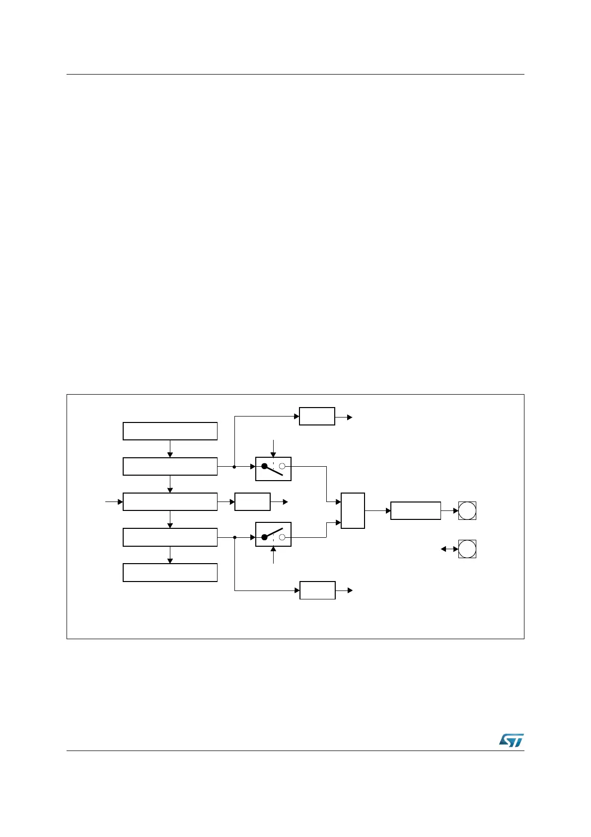
Figure 142. Double register compare mode block diagram
In this configuration example, the same timer allocation was chosen for both compare
registers, but each register may also be individually allocated to one of the two timers of the
respective CAPCOM unit. An example of this compare mode is shown in Figure 143. The
compare values in registers CCx and CCz are not modified.
Compare Register CCx
Comparator
CAPCOM Timer Ty
Comparator
Compare Register CCz
Input
Clock
TyIR
Mode 0
CCMODz
CCzIR
Interrupt
Request
Interrupt
Request
≥ 1
CCMODx
Mode 1
Toggle
Port Latch
CCxIO
CCxIO
x = 23...16, 7...0
y = 0, 1, 7, 8
z = 31...24, 15...8
CCxIR
Interrupt
Request