The external bus interface UM0404
196/564 DocID13284 Rev 2
drive it low again. If, however, the peripheral deactivates READY/READY after the first
sample point of the ST10F276, the controller samples an active READY/READY
and
terminates the current bus cycle, which, of course, is too early. By inserting predefined
wait-states the first READY/READY
sample point can be shifted to a time, where the
peripheral has safely controlled the READY/READY
line (after two wait-states in the
Figure 66).
8.3.7 Programmable chip select timing control
The position of the CS lines can be changed. By default (after reset), the CS lines change
half a CPU clock cycle after the rising edge of ALE. With the CSCFG bit set in the SYSCON
register, the CS
lines change with the rising edge of ALE, therefore the CS lines change at
the same time that the address lines are changed.
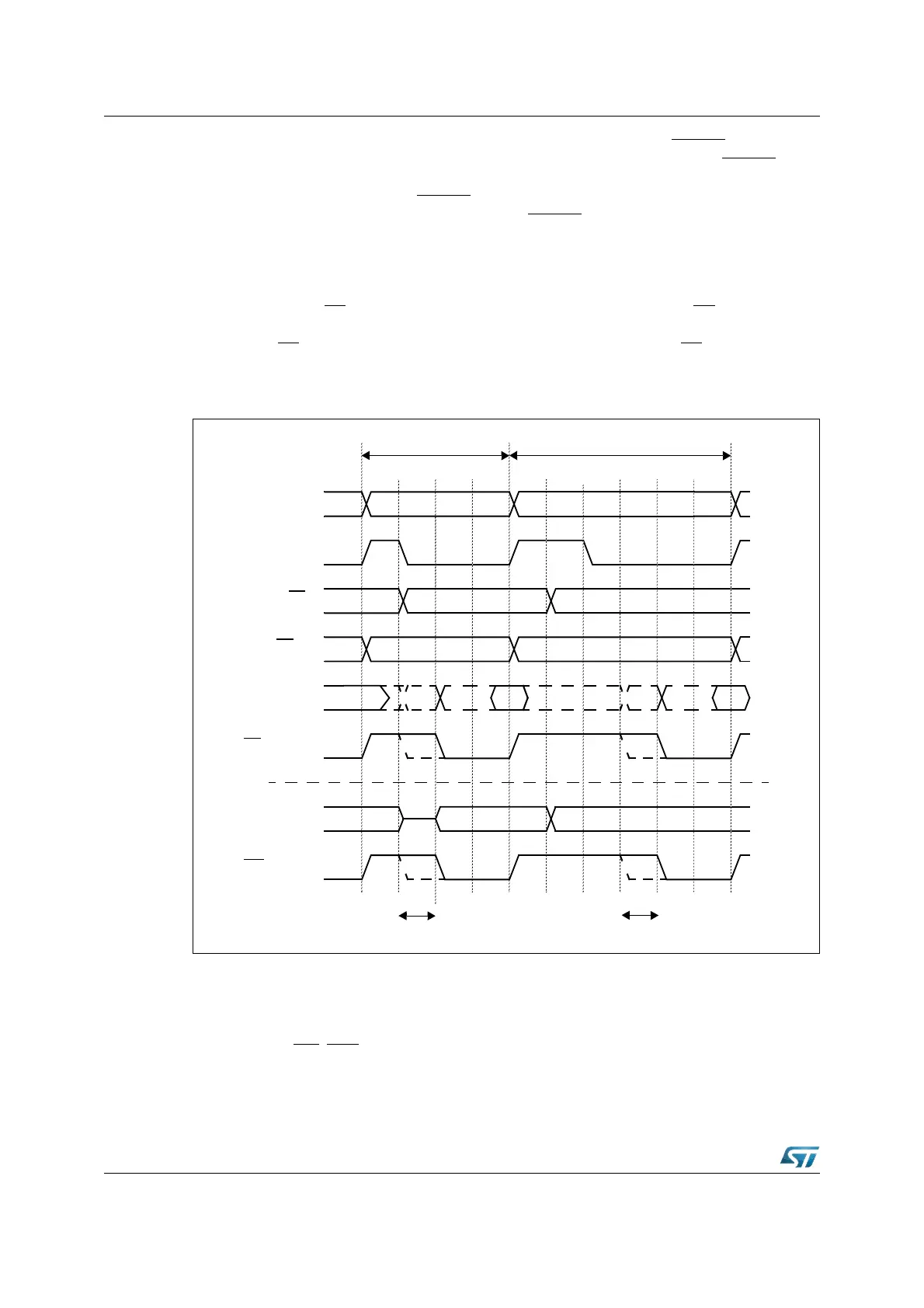
Figure 67. Chip select delay
8.4 Controlling the external bus controller
A set of registers controls the functions of the EBC. General features like the usage of
interface pins (WR
, BHE), segmentation and internal Memory mapping are controlled by the
SYSCON register.
Normal CS
RD
Address (P1)
ALE
Segment (P4)
Normal De-multiplexed
Bus Cycle
ALE Lengthen De-multiplexed
Bus Cycle
Early CS
WR
Read/Write
Delay
Data Data
Data
Data
BUS (P0)
BUS (P0)
Read/Write
Delay